
User guide


Table Of Contents
- Cyclone V Hard IP for PCI Express User Guide
- Contents
- 1. Datasheet
- 2. Getting Started with the Cyclone V Hard IP for PCI Express
- 3. Getting Started with the Avalon-MM Cyclone Hard IP for PCI Express
- Running Qsys
- Customizing the Cyclone VHard IP for PCI Express IP Core
- Adding the Remaining Components to the Qsys System
- Completing the Connections in Qsys
- Specifying Clocks and Interrupts
- Specifying Exported Interfaces
- Specifying Address Assignments
- Simulating the Example Design
- Simulating the Single DWord Design
- Understanding Channel Placement Guidelines
- Adding Synopsis Design Constraints
- Creating a Quartus II Project
- Compiling the Design
- Programming a Device
- 4. Parameter Settings for the Cyclone V Hard IP for PCI Express
- 5. Parameter Settings for the Avalon-MM Cyclone V Hard IP for PCI Express
- 6. IP Core Architecture
- Key Interfaces
- Protocol Layers
- Multi-Function Support
- PCI Express Avalon-MM Bridge
- Avalon-MM Bridge TLPs
- Avalon-MM-to-PCI Express Write Requests
- Avalon-MM-to-PCI Express Upstream Read Requests
- PCI Express-to-Avalon-MM Read Completions
- PCI Express-to-Avalon-MM Downstream Write Requests
- PCI Express-to-Avalon-MM Downstream Read Requests
- Avalon-MM-to-PCI Express Read Completions
- PCI Express-to-Avalon-MM Address Translation for Endpoints
- Minimizing BAR Sizes and the PCIe Address Space
- Avalon-MM-to-PCI Express Address Translation Algorithm
- Single DWord Completer Endpoint
- 7. IP Core Interfaces
- Cyclone V Hard IP for PCI Express
- Avalon-MM Hard IP for PCI Express
- Physical Layer Interface Signals
- Test Signals
- 8. Register Descriptions
- Configuration Space Register Content
- Altera-Defined Vendor Specific Extended Capability (VSEC)
- PCI Express Avalon-MM Bridge Control Register Access Content
- Avalon-MM to PCI Express Interrupt Registers
- PCI Express Mailbox Registers
- Avalon-MM-to-PCI Express Address Translation Table
- Root Port TLP Data Registers
- Programming Model for Avalon-MM Root Port
- PCI Express to Avalon-MM Interrupt Status and Enable Registers for Root Ports
- PCI Express to Avalon-MM Interrupt Status and Enable Registers for Endpoints
- Avalon-MM Mailbox Registers
- Correspondence between Configuration Space Registers and the PCIe Spec 2.1
- 9. Reset and Clocks
- 10. Transaction Layer Protocol (TLP) Details
- 11. Interrupts
- Interrupts for Endpoints Using the Avalon-ST Application Interface
- Interrupts for Root Ports Using the Avalon-ST Interface to the Application Layer
- Interrupts for Endpoints Using the Avalon-MM Interface to the Application Layer
- Interrupts for End Points Using the Avalon-MM Interface with Multiple MSI/MSI-X Support
- 12. Optional Features
- 13. Flow Control
- 14. Error Handling
- 15. Transceiver PHY IP Reconfiguration
- 16. SDC Timing Constraints
- 17. Testbench and Design Example
- Endpoint Testbench
- Root Port Testbench
- Chaining DMA Design Examples
- Test Driver Module
- Root Port Design Example
- Root Port BFM
- BFM Procedures and Functions
- 18. Debugging
- A. Transaction Layer Packet (TLP) Header Formats
- Additional Information
Chapter 17: Testbench and Design Example 17–19
Root Port Design Example
December 2013 Altera Corporation Cyclone V Hard IP for PCI Express
User Guide
■ Test Driver (altpcietb_bfm_driver_rp.v)—the chaining DMA Endpoint test driver
which configures the Root Port and Endpoint for DMA transfer and checks for the
successful transfer of data. Refer to the “Test Driver Module” on page 17–14 for a
detailed description.
You can use the example Root Port design for Verilog HDL simulation. All of the
modules necessary to implement the example design with the variation file are
contained in altpcietb_bfm_ep_example_chaining_pipen1b.v.
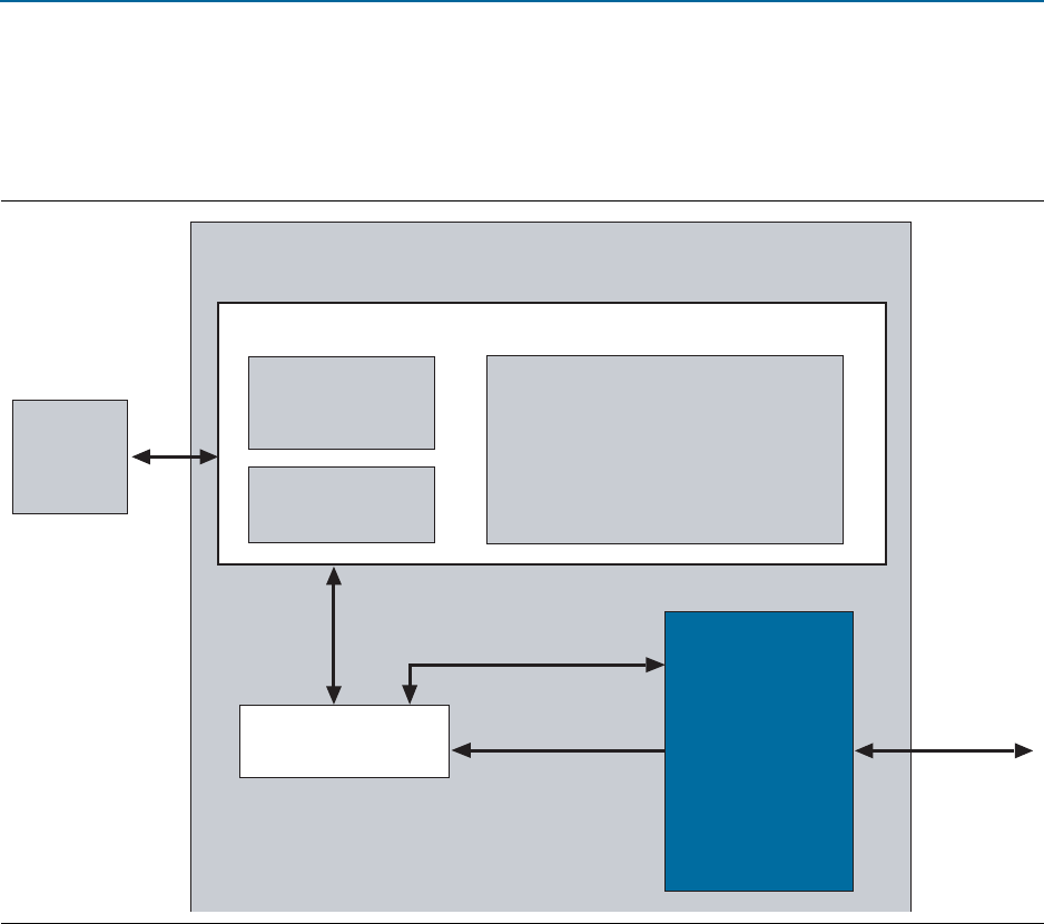
The top-level of the testbench instantiates the following key files:
■ altlpcietb_bfm_top_ep.v— this is the Endpoint BFM. This file also instantiates the
SERDES and PIPE interface.
■ altpcietb_pipe_phy.v—used to simulate the PIPE interface.
■ altpcietb_bfm_ep_example_chaining_pipen1b.v—the top-level of the Root Port
design example that you use for simulation. This module instantiates the Root Port
variation, <variation_name>.v, and the Root Port application
altpcietb_bfm_vc_intf_<application_width>. This module provides both PIPE and
serial interfaces for the simulation environment. This module has two debug ports
named
test_out
_
icm
(which is the
test_out
signal from the Hard IP) and
test_in
which allows you to monitor and control internal states of the Hard IP
variation. (Refer to “Test Signals” on page 7–54.)
Figure 17–3. Root Port Design Example
Root Port
Variation
(variation_name.v)
Avalon-ST Interface
(altpcietb_bfm_vc_intf)
Test Driver
(altpcietb_bfm_
driver_rp.v)
BFM Shared Memory
(altpcietb_bfm_shmem
_common)
BFM Read/Write Shared Request Procedures
BFM Configuration Procedures
BFM Request Interface
(altpcietb_bfm_req_intf_common)
BFM Log Interface
(altpcietb_bfm_log
_common)
PCI Express
Link
Root Port BFM Tasks and Shared Memory
altpcietb_bfm_ep_example_chaining_pipe1b.v
Avalon-ST