
User guide
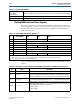
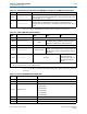
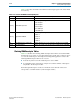
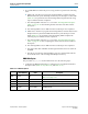
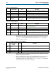
Table Of Contents
- Cyclone V Hard IP for PCI Express User Guide
- Contents
- 1. Datasheet
- 2. Getting Started with the Cyclone V Hard IP for PCI Express
- 3. Getting Started with the Avalon-MM Cyclone Hard IP for PCI Express
- Running Qsys
- Customizing the Cyclone VHard IP for PCI Express IP Core
- Adding the Remaining Components to the Qsys System
- Completing the Connections in Qsys
- Specifying Clocks and Interrupts
- Specifying Exported Interfaces
- Specifying Address Assignments
- Simulating the Example Design
- Simulating the Single DWord Design
- Understanding Channel Placement Guidelines
- Adding Synopsis Design Constraints
- Creating a Quartus II Project
- Compiling the Design
- Programming a Device
- 4. Parameter Settings for the Cyclone V Hard IP for PCI Express
- 5. Parameter Settings for the Avalon-MM Cyclone V Hard IP for PCI Express
- 6. IP Core Architecture
- Key Interfaces
- Protocol Layers
- Multi-Function Support
- PCI Express Avalon-MM Bridge
- Avalon-MM Bridge TLPs
- Avalon-MM-to-PCI Express Write Requests
- Avalon-MM-to-PCI Express Upstream Read Requests
- PCI Express-to-Avalon-MM Read Completions
- PCI Express-to-Avalon-MM Downstream Write Requests
- PCI Express-to-Avalon-MM Downstream Read Requests
- Avalon-MM-to-PCI Express Read Completions
- PCI Express-to-Avalon-MM Address Translation for Endpoints
- Minimizing BAR Sizes and the PCIe Address Space
- Avalon-MM-to-PCI Express Address Translation Algorithm
- Single DWord Completer Endpoint
- 7. IP Core Interfaces
- Cyclone V Hard IP for PCI Express
- Avalon-MM Hard IP for PCI Express
- Physical Layer Interface Signals
- Test Signals
- 8. Register Descriptions
- Configuration Space Register Content
- Altera-Defined Vendor Specific Extended Capability (VSEC)
- PCI Express Avalon-MM Bridge Control Register Access Content
- Avalon-MM to PCI Express Interrupt Registers
- PCI Express Mailbox Registers
- Avalon-MM-to-PCI Express Address Translation Table
- Root Port TLP Data Registers
- Programming Model for Avalon-MM Root Port
- PCI Express to Avalon-MM Interrupt Status and Enable Registers for Root Ports
- PCI Express to Avalon-MM Interrupt Status and Enable Registers for Endpoints
- Avalon-MM Mailbox Registers
- Correspondence between Configuration Space Registers and the PCIe Spec 2.1
- 9. Reset and Clocks
- 10. Transaction Layer Protocol (TLP) Details
- 11. Interrupts
- Interrupts for Endpoints Using the Avalon-ST Application Interface
- Interrupts for Root Ports Using the Avalon-ST Interface to the Application Layer
- Interrupts for Endpoints Using the Avalon-MM Interface to the Application Layer
- Interrupts for End Points Using the Avalon-MM Interface with Multiple MSI/MSI-X Support
- 12. Optional Features
- 13. Flow Control
- 14. Error Handling
- 15. Transceiver PHY IP Reconfiguration
- 16. SDC Timing Constraints
- 17. Testbench and Design Example
- Endpoint Testbench
- Root Port Testbench
- Chaining DMA Design Examples
- Test Driver Module
- Root Port Design Example
- Root Port BFM
- BFM Procedures and Functions
- 18. Debugging
- A. Transaction Layer Packet (TLP) Header Formats
- Additional Information
Chapter 17: Testbench and Design Example 17–17
Test Driver Module
December 2013 Altera Corporation Cyclone V Hard IP for PCI Express
User Guide
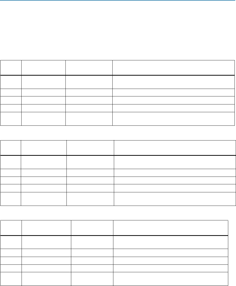
DMA Read Cycles
The procedure
dma_rd_test
used for DMA read uses the following three steps:
1. Configures the BFM shared memory with a call to the procedure
dma_set_rd_desc_data
which sets three descriptor tables (Table 17–15,
Table 17–16, and Table 17–17).
Table 17–15. Read Descriptor 0
Offset in BFM
Shared Memory
Value Description
DW0 0x910 82
Transfer length in dwords and control bits as described in on
page 17–14
DW1 0x914 3 Endpoint address value
DW2 0x918 0 BFM shared memory data buffer 0 upper address value
DW3 0x91c 0x8DF0 BFM shared memory data buffer 0 lower address value
Data
Buffer 0
0x8DF0
Increment by 1 from
0xAAA0_0001
Data content in the BFM shared memory from address: 0x89F0
Table 17–16. Read Descriptor 1
Offset in BFM
Shared Memory
Value Description
DW0 0x920 1,024
Transfer length in dwords and control bits as described in on
page 17–14
DW1 0x924 0 Endpoint address value
DW2 0x928 10 BFM shared memory data buffer 1 upper address value
DW3 0x92c 0x10900 BFM shared memory data buffer 1 lower address value
Data
Buffer 1
0x10900
Increment by 1 from
0xBBBB_0001
Data content in the BFM shared memory from address:
0x10900
Table 17–17. Read Descriptor 2
Offset in BFM Shared
Memory
Value Description
DW0 0x930 644
Transfer length in dwords and control bits as described in
on page 17–14
DW1 0x934 0 Endpoint address value
DW2 0x938 0 BFM shared memory upper address value
DW3 0x93c 0x20EF0 BFM shared memory lower address value
Data
Buffer 2
0x20EF0
Increment by 1 from
0xCCCC_0001
Data content in the BFM shared memory from address:
0x20EF0