
User guide
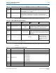
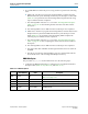
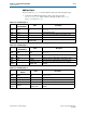
Table Of Contents
- Cyclone V Hard IP for PCI Express User Guide
- Contents
- 1. Datasheet
- 2. Getting Started with the Cyclone V Hard IP for PCI Express
- 3. Getting Started with the Avalon-MM Cyclone Hard IP for PCI Express
- Running Qsys
- Customizing the Cyclone VHard IP for PCI Express IP Core
- Adding the Remaining Components to the Qsys System
- Completing the Connections in Qsys
- Specifying Clocks and Interrupts
- Specifying Exported Interfaces
- Specifying Address Assignments
- Simulating the Example Design
- Simulating the Single DWord Design
- Understanding Channel Placement Guidelines
- Adding Synopsis Design Constraints
- Creating a Quartus II Project
- Compiling the Design
- Programming a Device
- 4. Parameter Settings for the Cyclone V Hard IP for PCI Express
- 5. Parameter Settings for the Avalon-MM Cyclone V Hard IP for PCI Express
- 6. IP Core Architecture
- Key Interfaces
- Protocol Layers
- Multi-Function Support
- PCI Express Avalon-MM Bridge
- Avalon-MM Bridge TLPs
- Avalon-MM-to-PCI Express Write Requests
- Avalon-MM-to-PCI Express Upstream Read Requests
- PCI Express-to-Avalon-MM Read Completions
- PCI Express-to-Avalon-MM Downstream Write Requests
- PCI Express-to-Avalon-MM Downstream Read Requests
- Avalon-MM-to-PCI Express Read Completions
- PCI Express-to-Avalon-MM Address Translation for Endpoints
- Minimizing BAR Sizes and the PCIe Address Space
- Avalon-MM-to-PCI Express Address Translation Algorithm
- Single DWord Completer Endpoint
- 7. IP Core Interfaces
- Cyclone V Hard IP for PCI Express
- Avalon-MM Hard IP for PCI Express
- Physical Layer Interface Signals
- Test Signals
- 8. Register Descriptions
- Configuration Space Register Content
- Altera-Defined Vendor Specific Extended Capability (VSEC)
- PCI Express Avalon-MM Bridge Control Register Access Content
- Avalon-MM to PCI Express Interrupt Registers
- PCI Express Mailbox Registers
- Avalon-MM-to-PCI Express Address Translation Table
- Root Port TLP Data Registers
- Programming Model for Avalon-MM Root Port
- PCI Express to Avalon-MM Interrupt Status and Enable Registers for Root Ports
- PCI Express to Avalon-MM Interrupt Status and Enable Registers for Endpoints
- Avalon-MM Mailbox Registers
- Correspondence between Configuration Space Registers and the PCIe Spec 2.1
- 9. Reset and Clocks
- 10. Transaction Layer Protocol (TLP) Details
- 11. Interrupts
- Interrupts for Endpoints Using the Avalon-ST Application Interface
- Interrupts for Root Ports Using the Avalon-ST Interface to the Application Layer
- Interrupts for Endpoints Using the Avalon-MM Interface to the Application Layer
- Interrupts for End Points Using the Avalon-MM Interface with Multiple MSI/MSI-X Support
- 12. Optional Features
- 13. Flow Control
- 14. Error Handling
- 15. Transceiver PHY IP Reconfiguration
- 16. SDC Timing Constraints
- 17. Testbench and Design Example
- Endpoint Testbench
- Root Port Testbench
- Chaining DMA Design Examples
- Test Driver Module
- Root Port Design Example
- Root Port BFM
- BFM Procedures and Functions
- 18. Debugging
- A. Transaction Layer Packet (TLP) Header Formats
- Additional Information

17–14 Chapter 17: Testbench and Design Example
Test Driver Module
Cyclone V Hard IP for PCI Express December 2013 Altera Corporation
User Guide
Each descriptor provides the hardware information on one DMA transfer. Table 17–10
describes each descriptor field.
Test Driver Module
The BFM driver module, altpcietb_bfm_driver_chaining.v is configured to test the
chaining DMA example Endpoint design. The BFM driver module configures the
Endpoint Configuration Space registers and then tests the example Endpoint chaining
DMA channel. This file is stored in the
<working_dir>testbench/<variation_name>/simulation/submodules directory.
The BFM test driver module performs the following steps in sequence:
1. Configures the Root Port and Endpoint Configuration Spaces, which the BFM test
driver module does by calling the procedure
ebfm_cfg_rp_ep
, which is part of
altpcietb_bfm_configure.
2. Finds a suitable BAR to access the example Endpoint design Control Register
space. Either BARs 2 or 3 must be at least a 256-byte memory BAR to perform the
DMA channel test. The
find_mem_bar
procedure in the
altpcietb_bfm_driver_chaining does this.
Table 17–10. Chaining DMA Descriptor Fields
Descriptor Field
Endpoint
Access
RC Access Description
Endpoint Address R R/W
A 32-bit field that specifies the base address of the memory transfer on the
Endpoint site.
RC Address
Upper DWORD
R R/W Specifies the upper base address of the memory transfer on the RC site.
RC Address
Lower DWORD
R R/W Specifies the lower base address of the memory transfer on the RC site.
DMA Length R R/W Specifies the number of DMA DWORDs to transfer.
EPLAST_ENA
RR/W
This bit is
OR
’d with the
EPLAST_ENA
bit of the control register. When
EPLAST_ENA
is set, the Endpoint DMA module updates the EPLAST field of
the descriptor table with the number of the last completed descriptor, in the
form <0 – n>. (Refer to Table 17–7.)
MSI_ENA
RR/W
This bit is
OR
’d with the
MSI
bit of the descriptor header. When this bit is set
the Endpoint DMA module sends an interrupt when the descriptor is
completed.