
User guide
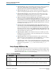
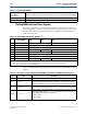
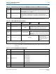
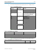
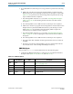
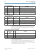
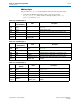
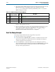
Table Of Contents
- Cyclone V Hard IP for PCI Express User Guide
- Contents
- 1. Datasheet
- 2. Getting Started with the Cyclone V Hard IP for PCI Express
- 3. Getting Started with the Avalon-MM Cyclone Hard IP for PCI Express
- Running Qsys
- Customizing the Cyclone VHard IP for PCI Express IP Core
- Adding the Remaining Components to the Qsys System
- Completing the Connections in Qsys
- Specifying Clocks and Interrupts
- Specifying Exported Interfaces
- Specifying Address Assignments
- Simulating the Example Design
- Simulating the Single DWord Design
- Understanding Channel Placement Guidelines
- Adding Synopsis Design Constraints
- Creating a Quartus II Project
- Compiling the Design
- Programming a Device
- 4. Parameter Settings for the Cyclone V Hard IP for PCI Express
- 5. Parameter Settings for the Avalon-MM Cyclone V Hard IP for PCI Express
- 6. IP Core Architecture
- Key Interfaces
- Protocol Layers
- Multi-Function Support
- PCI Express Avalon-MM Bridge
- Avalon-MM Bridge TLPs
- Avalon-MM-to-PCI Express Write Requests
- Avalon-MM-to-PCI Express Upstream Read Requests
- PCI Express-to-Avalon-MM Read Completions
- PCI Express-to-Avalon-MM Downstream Write Requests
- PCI Express-to-Avalon-MM Downstream Read Requests
- Avalon-MM-to-PCI Express Read Completions
- PCI Express-to-Avalon-MM Address Translation for Endpoints
- Minimizing BAR Sizes and the PCIe Address Space
- Avalon-MM-to-PCI Express Address Translation Algorithm
- Single DWord Completer Endpoint
- 7. IP Core Interfaces
- Cyclone V Hard IP for PCI Express
- Avalon-MM Hard IP for PCI Express
- Physical Layer Interface Signals
- Test Signals
- 8. Register Descriptions
- Configuration Space Register Content
- Altera-Defined Vendor Specific Extended Capability (VSEC)
- PCI Express Avalon-MM Bridge Control Register Access Content
- Avalon-MM to PCI Express Interrupt Registers
- PCI Express Mailbox Registers
- Avalon-MM-to-PCI Express Address Translation Table
- Root Port TLP Data Registers
- Programming Model for Avalon-MM Root Port
- PCI Express to Avalon-MM Interrupt Status and Enable Registers for Root Ports
- PCI Express to Avalon-MM Interrupt Status and Enable Registers for Endpoints
- Avalon-MM Mailbox Registers
- Correspondence between Configuration Space Registers and the PCIe Spec 2.1
- 9. Reset and Clocks
- 10. Transaction Layer Protocol (TLP) Details
- 11. Interrupts
- Interrupts for Endpoints Using the Avalon-ST Application Interface
- Interrupts for Root Ports Using the Avalon-ST Interface to the Application Layer
- Interrupts for Endpoints Using the Avalon-MM Interface to the Application Layer
- Interrupts for End Points Using the Avalon-MM Interface with Multiple MSI/MSI-X Support
- 12. Optional Features
- 13. Flow Control
- 14. Error Handling
- 15. Transceiver PHY IP Reconfiguration
- 16. SDC Timing Constraints
- 17. Testbench and Design Example
- Endpoint Testbench
- Root Port Testbench
- Chaining DMA Design Examples
- Test Driver Module
- Root Port Design Example
- Root Port BFM
- BFM Procedures and Functions
- 18. Debugging
- A. Transaction Layer Packet (TLP) Header Formats
- Additional Information
Chapter 17: Testbench and Design Example 17–13
Chaining DMA Design Examples
December 2013 Altera Corporation Cyclone V Hard IP for PCI Express
User Guide
1 Note that the chaining DMA descriptor table should not cross a 4 KByte boundary.
Table 17–8 shows the layout of the descriptor fields following the descriptor header.
Table 17–9 shows the layout of the control fields of the chaining DMA descriptor.
Table 17–7. Chaining DMA Descriptor Table
Byte Address Offset to
Base Source
Descriptor Type Description
0x0
Descriptor Header
Reserved
0x4 Reserved
0x8 Reserved
0xC
EPLAST - when enabled by the
EPLAST_ENA
bit
in the control register or descriptor, this location
records the number of the last descriptor
completed by the chaining DMA module.
0x10
Descriptor 0
Control fields, DMA length
0x14 Endpoint address
0x18 RC address upper dword
0x1C RC address lower dword
0x20
Descriptor 1
Control fields, DMA length
0x24 Endpoint address
0x28 RC address upper dword
0x2C RC address lower dword
. . .
0x ..0
Descriptor <n>
Control fields, DMA length
0x ..4 Endpoint address
0x ..8 RC address upper dword
0x ..C RC address lower dword
Table 17–8. Chaining DMA Descriptor Format Map
3122 21 16 150
Reserved Control Fields (refer to Table 17–9) DMA Length
Endpoint Address
RC Address Upper DWORD
RC Address Lower DWORD
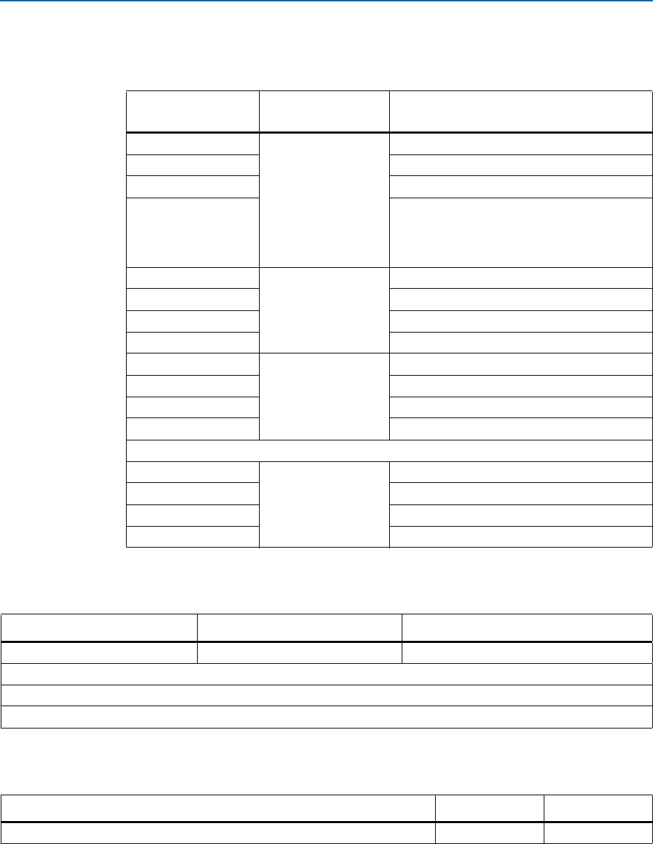
Table 17–9. Chaining DMA Descriptor Format Map (Control Fields)
2118 17 16
Reserved
EPLAST_ENA MSI