
User guide
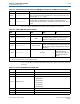
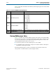
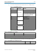
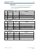
Table Of Contents
- Cyclone V Hard IP for PCI Express User Guide
- Contents
- 1. Datasheet
- 2. Getting Started with the Cyclone V Hard IP for PCI Express
- 3. Getting Started with the Avalon-MM Cyclone Hard IP for PCI Express
- Running Qsys
- Customizing the Cyclone VHard IP for PCI Express IP Core
- Adding the Remaining Components to the Qsys System
- Completing the Connections in Qsys
- Specifying Clocks and Interrupts
- Specifying Exported Interfaces
- Specifying Address Assignments
- Simulating the Example Design
- Simulating the Single DWord Design
- Understanding Channel Placement Guidelines
- Adding Synopsis Design Constraints
- Creating a Quartus II Project
- Compiling the Design
- Programming a Device
- 4. Parameter Settings for the Cyclone V Hard IP for PCI Express
- 5. Parameter Settings for the Avalon-MM Cyclone V Hard IP for PCI Express
- 6. IP Core Architecture
- Key Interfaces
- Protocol Layers
- Multi-Function Support
- PCI Express Avalon-MM Bridge
- Avalon-MM Bridge TLPs
- Avalon-MM-to-PCI Express Write Requests
- Avalon-MM-to-PCI Express Upstream Read Requests
- PCI Express-to-Avalon-MM Read Completions
- PCI Express-to-Avalon-MM Downstream Write Requests
- PCI Express-to-Avalon-MM Downstream Read Requests
- Avalon-MM-to-PCI Express Read Completions
- PCI Express-to-Avalon-MM Address Translation for Endpoints
- Minimizing BAR Sizes and the PCIe Address Space
- Avalon-MM-to-PCI Express Address Translation Algorithm
- Single DWord Completer Endpoint
- 7. IP Core Interfaces
- Cyclone V Hard IP for PCI Express
- Avalon-MM Hard IP for PCI Express
- Physical Layer Interface Signals
- Test Signals
- 8. Register Descriptions
- Configuration Space Register Content
- Altera-Defined Vendor Specific Extended Capability (VSEC)
- PCI Express Avalon-MM Bridge Control Register Access Content
- Avalon-MM to PCI Express Interrupt Registers
- PCI Express Mailbox Registers
- Avalon-MM-to-PCI Express Address Translation Table
- Root Port TLP Data Registers
- Programming Model for Avalon-MM Root Port
- PCI Express to Avalon-MM Interrupt Status and Enable Registers for Root Ports
- PCI Express to Avalon-MM Interrupt Status and Enable Registers for Endpoints
- Avalon-MM Mailbox Registers
- Correspondence between Configuration Space Registers and the PCIe Spec 2.1
- 9. Reset and Clocks
- 10. Transaction Layer Protocol (TLP) Details
- 11. Interrupts
- Interrupts for Endpoints Using the Avalon-ST Application Interface
- Interrupts for Root Ports Using the Avalon-ST Interface to the Application Layer
- Interrupts for Endpoints Using the Avalon-MM Interface to the Application Layer
- Interrupts for End Points Using the Avalon-MM Interface with Multiple MSI/MSI-X Support
- 12. Optional Features
- 13. Flow Control
- 14. Error Handling
- 15. Transceiver PHY IP Reconfiguration
- 16. SDC Timing Constraints
- 17. Testbench and Design Example
- Endpoint Testbench
- Root Port Testbench
- Chaining DMA Design Examples
- Test Driver Module
- Root Port Design Example
- Root Port BFM
- BFM Procedures and Functions
- 18. Debugging
- A. Transaction Layer Packet (TLP) Header Formats
- Additional Information

Chapter 17: Testbench and Design Example 17–9
Chaining DMA Design Examples
December 2013 Altera Corporation Cyclone V Hard IP for PCI Express
User Guide
■ altpcierd_dma_dt—This module arbitrates PCI Express packets issued by the
submodules altpcierd_dma_prg_reg, altpcierd_read_dma_requester,
altpcierd_write_dma_requester and altpcierd_dma_descriptor.
■ altpcierd_dma_prg_reg—This module contains the chaining DMA control
registers which get programmed by the software application or BFM driver.
■ altpcierd_dma_descriptor—This module retrieves the DMA read or write
descriptor from the BFM shared memory, and stores it in a descriptor FIFO.
This module issues upstream PCI Express TLPs of type Mrd.
■ altpcierd_read_dma_requester, altpcierd_read_dma_requester_128—For each
descriptor located in the altpcierd_descriptor FIFO, this module transfers data
from the BFM shared memory to the Endpoint memory by issuing MRd PCI
Express transaction layer packets. altpcierd_read_dma_requester is used with
the 64-bit Avalon-ST IP core. altpcierd_read_dma_requester_128 is used with
the 128-bit Avalon-ST IP core.
■ altpcierd_write_dma_requester, altpcierd_write_dma_requester_128—For
each descriptor located in the altpcierd_descriptor FIFO, this module transfers
data from the Endpoint memory to the BFM shared memory by issuing MWr
PCI Express transaction layer packets. altpcierd_write_dma_requester is used
with the 64-bit Avalon-ST IP core. altpcierd_write_dma_requester_128 is used
with the 128-bit Avalon-ST IP core.ls
■ altpcierd_cpld_rx_buffer—This modules monitors the available space of the
RX Buffer; It prevents RX Buffer overflow by arbitrating memory read request
issued by the Application Layer.
■ altpcierd_cplerr_lmi—This module transfers the err_desc_func0 from the
Application Layer to the Hard IP block using the LMI interface. It also retimes
the
cpl_er
r bits from the Application Layer to the Hard IP block.
■ altpcierd_tl_cfg_sample—This module demultiplexes the Configuration Space
signals from the
tl_cfg_ctl
bus from the Hard IP block and synchronizes this
information, along with the
tl_cfg_sts
bus to the user clock (
pld_clk
)
domain.
Design Example BAR/Address Map
The design example maps received memory transactions to either the target memory
block or the control register block based on which BAR the transaction matches. There
are multiple BARs that map to each of these blocks to maximize interoperability with
different variation files. Table 17–1 shows the mapping.
Table 17–1. Design Example BAR Map
Memory BAR Mapping
32-bit BAR0
32-bit BAR1
64-bit BAR1:0
Maps to 32 KByte target memory block. Use the rc_slave module to bypass the chaining DMA.
32-bit BAR2
32-bit BAR3
64-bit BAR3:2
Maps to DMA Read and DMA write control and status registers, a minimum of 256 bytes.