
User guide

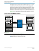
Table Of Contents
- Cyclone V Hard IP for PCI Express User Guide
- Contents
- 1. Datasheet
- 2. Getting Started with the Cyclone V Hard IP for PCI Express
- 3. Getting Started with the Avalon-MM Cyclone Hard IP for PCI Express
- Running Qsys
- Customizing the Cyclone VHard IP for PCI Express IP Core
- Adding the Remaining Components to the Qsys System
- Completing the Connections in Qsys
- Specifying Clocks and Interrupts
- Specifying Exported Interfaces
- Specifying Address Assignments
- Simulating the Example Design
- Simulating the Single DWord Design
- Understanding Channel Placement Guidelines
- Adding Synopsis Design Constraints
- Creating a Quartus II Project
- Compiling the Design
- Programming a Device
- 4. Parameter Settings for the Cyclone V Hard IP for PCI Express
- 5. Parameter Settings for the Avalon-MM Cyclone V Hard IP for PCI Express
- 6. IP Core Architecture
- Key Interfaces
- Protocol Layers
- Multi-Function Support
- PCI Express Avalon-MM Bridge
- Avalon-MM Bridge TLPs
- Avalon-MM-to-PCI Express Write Requests
- Avalon-MM-to-PCI Express Upstream Read Requests
- PCI Express-to-Avalon-MM Read Completions
- PCI Express-to-Avalon-MM Downstream Write Requests
- PCI Express-to-Avalon-MM Downstream Read Requests
- Avalon-MM-to-PCI Express Read Completions
- PCI Express-to-Avalon-MM Address Translation for Endpoints
- Minimizing BAR Sizes and the PCIe Address Space
- Avalon-MM-to-PCI Express Address Translation Algorithm
- Single DWord Completer Endpoint
- 7. IP Core Interfaces
- Cyclone V Hard IP for PCI Express
- Avalon-MM Hard IP for PCI Express
- Physical Layer Interface Signals
- Test Signals
- 8. Register Descriptions
- Configuration Space Register Content
- Altera-Defined Vendor Specific Extended Capability (VSEC)
- PCI Express Avalon-MM Bridge Control Register Access Content
- Avalon-MM to PCI Express Interrupt Registers
- PCI Express Mailbox Registers
- Avalon-MM-to-PCI Express Address Translation Table
- Root Port TLP Data Registers
- Programming Model for Avalon-MM Root Port
- PCI Express to Avalon-MM Interrupt Status and Enable Registers for Root Ports
- PCI Express to Avalon-MM Interrupt Status and Enable Registers for Endpoints
- Avalon-MM Mailbox Registers
- Correspondence between Configuration Space Registers and the PCIe Spec 2.1
- 9. Reset and Clocks
- 10. Transaction Layer Protocol (TLP) Details
- 11. Interrupts
- Interrupts for Endpoints Using the Avalon-ST Application Interface
- Interrupts for Root Ports Using the Avalon-ST Interface to the Application Layer
- Interrupts for Endpoints Using the Avalon-MM Interface to the Application Layer
- Interrupts for End Points Using the Avalon-MM Interface with Multiple MSI/MSI-X Support
- 12. Optional Features
- 13. Flow Control
- 14. Error Handling
- 15. Transceiver PHY IP Reconfiguration
- 16. SDC Timing Constraints
- 17. Testbench and Design Example
- Endpoint Testbench
- Root Port Testbench
- Chaining DMA Design Examples
- Test Driver Module
- Root Port Design Example
- Root Port BFM
- BFM Procedures and Functions
- 18. Debugging
- A. Transaction Layer Packet (TLP) Header Formats
- Additional Information

17–4 Chapter 17: Testbench and Design Example
Chaining DMA Design Examples
Cyclone V Hard IP for PCI Express December 2013 Altera Corporation
User Guide
1 One parameter,
serial_sim_hwtcl
, in the altprice_tbed_sv_hwtcl.v file, controls
whether the testbench simulates in PIPE mode or serial mode. When is set to 0, the
simulation runs in PIPE mode; otherwise, it runs in serial mode.
Chaining DMA Design Examples
This design examples shows how to create a chaining DMA Native Endpoint which
supports simultaneous DMA read and write transactions. The write DMA module
implements write operations from the Endpoint memory to the root complex (RC)
memory. The read DMA implements read operations from the RC memory to the
Endpoint memory.
When operating on a hardware platform, the DMA is typically controlled by a
software application running on the root complex processor. In simulation, the
generated testbench, along with this design example, provides a BFM driver module
in Verilog HDL that controls the DMA operations. Because the example relies on no
other hardware interface than the PCI Express link, you can use the design example
for the initial hardware validation of your system.
The design example includes the following two main components:
■ The Root Port variation
■ An Application Layer design example
The end point or Root Port variant is generated in the language (Verilog HDL or
VHDL) that you selected for the variation file. The testbench files are only generated
in Verilog HDL in the current release. If you choose to use VHDL for your variant, you
must have a mixed-language simulator to run this testbench.
1 The chaining DMA design example requires setting BAR 2 or BAR 3 to a minimum of
256 bytes. To run the DMA tests using MSI, you must set the Number of MSI
messages requested parameter under the PCI Express/PCI Capabilities page to at
least 2.
The chaining DMA design example uses an architecture capable of transferring a
large amount of fragmented memory without accessing the DMA registers for every
memory block. For each block of memory to be transferred, the chaining DMA design
example uses a descriptor table containing the following information:
■ Length of the transfer
■ Address of the source
■ Address of the destination
■ Control bits to set the handshaking behavior between the software application or
BFM driver and the chaining DMA module
1 The chaining DMA design example only supports dword-aligned accesses. The
chaining DMA design example does not support ECRC forwarding for Cyclone V.