
User guide


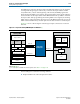


Table Of Contents
- Cyclone V Hard IP for PCI Express User Guide
- Contents
- 1. Datasheet
- 2. Getting Started with the Cyclone V Hard IP for PCI Express
- 3. Getting Started with the Avalon-MM Cyclone Hard IP for PCI Express
- Running Qsys
- Customizing the Cyclone VHard IP for PCI Express IP Core
- Adding the Remaining Components to the Qsys System
- Completing the Connections in Qsys
- Specifying Clocks and Interrupts
- Specifying Exported Interfaces
- Specifying Address Assignments
- Simulating the Example Design
- Simulating the Single DWord Design
- Understanding Channel Placement Guidelines
- Adding Synopsis Design Constraints
- Creating a Quartus II Project
- Compiling the Design
- Programming a Device
- 4. Parameter Settings for the Cyclone V Hard IP for PCI Express
- 5. Parameter Settings for the Avalon-MM Cyclone V Hard IP for PCI Express
- 6. IP Core Architecture
- Key Interfaces
- Protocol Layers
- Multi-Function Support
- PCI Express Avalon-MM Bridge
- Avalon-MM Bridge TLPs
- Avalon-MM-to-PCI Express Write Requests
- Avalon-MM-to-PCI Express Upstream Read Requests
- PCI Express-to-Avalon-MM Read Completions
- PCI Express-to-Avalon-MM Downstream Write Requests
- PCI Express-to-Avalon-MM Downstream Read Requests
- Avalon-MM-to-PCI Express Read Completions
- PCI Express-to-Avalon-MM Address Translation for Endpoints
- Minimizing BAR Sizes and the PCIe Address Space
- Avalon-MM-to-PCI Express Address Translation Algorithm
- Single DWord Completer Endpoint
- 7. IP Core Interfaces
- Cyclone V Hard IP for PCI Express
- Avalon-MM Hard IP for PCI Express
- Physical Layer Interface Signals
- Test Signals
- 8. Register Descriptions
- Configuration Space Register Content
- Altera-Defined Vendor Specific Extended Capability (VSEC)
- PCI Express Avalon-MM Bridge Control Register Access Content
- Avalon-MM to PCI Express Interrupt Registers
- PCI Express Mailbox Registers
- Avalon-MM-to-PCI Express Address Translation Table
- Root Port TLP Data Registers
- Programming Model for Avalon-MM Root Port
- PCI Express to Avalon-MM Interrupt Status and Enable Registers for Root Ports
- PCI Express to Avalon-MM Interrupt Status and Enable Registers for Endpoints
- Avalon-MM Mailbox Registers
- Correspondence between Configuration Space Registers and the PCIe Spec 2.1
- 9. Reset and Clocks
- 10. Transaction Layer Protocol (TLP) Details
- 11. Interrupts
- Interrupts for Endpoints Using the Avalon-ST Application Interface
- Interrupts for Root Ports Using the Avalon-ST Interface to the Application Layer
- Interrupts for Endpoints Using the Avalon-MM Interface to the Application Layer
- Interrupts for End Points Using the Avalon-MM Interface with Multiple MSI/MSI-X Support
- 12. Optional Features
- 13. Flow Control
- 14. Error Handling
- 15. Transceiver PHY IP Reconfiguration
- 16. SDC Timing Constraints
- 17. Testbench and Design Example
- Endpoint Testbench
- Root Port Testbench
- Chaining DMA Design Examples
- Test Driver Module
- Root Port Design Example
- Root Port BFM
- BFM Procedures and Functions
- 18. Debugging
- A. Transaction Layer Packet (TLP) Header Formats
- Additional Information

Chapter 17: Testbench and Design Example 17–3
Root Port Testbench
December 2013 Altera Corporation Cyclone V Hard IP for PCI Express
User Guide
■ <qsys_systemname>— This is the example Endpoint design. For more
information about this module, refer to “Chaining DMA Design Examples” on
page 17–4.
■ altpcietb_bfm_top_rp.v—This is the Root Port PCI Express BFM. For more
information about this module, refer to“Root Port BFM” on page 17–20.
■ altpcietb_pipe_phy—There are eight instances of this module, one per lane. These
modules interconnect the PIPE MAC layer interfaces of the Root Port and the
Endpoint. The module mimics the behavior of the PIPE PHY layer to both MAC
interfaces.
■ altpcietb_bfm_driver_chaining—This module drives transactions to the Root
Port BFM. This is the module that you modify to vary the transactions sent to the
example Endpoint design or your own design. For more information about this
module, refer to “Root Port Design Example” on page 17–18.
In addition, the testbench has routines that perform the following tasks:
■ Generates the reference clock for the Endpoint at the required frequency.
■ Provides a PCI Express reset at start up.
1 One parameter,
serial_sim_hwtcl
, in the altprice_tbed_sv_hwtcl.v file, controls
whether the testbench simulates in PIPE mode or serial mode. When is set to 0, the
simulation runs in PIPE mode; when set to 1, it runs in serial mode.
Root Port Testbench
This testbench simulates up to an ×8 PCI Express link using either the PIPE interfaces
of the Root Port and Endpoints or the serial PCI Express interface. The testbench
design does not allow more than one PCI Express link to be simulated at a time. The
top-level of the testbench instantiates four main modules:
■ <qsys_systemname>— Name of Root Port This is the example Root Port design. For
more information about this module, refer to “Root Port Design Example” on
page 17–18.
■ altpcietb_bfm_ep_example_chaining_pipen1b—This is the Endpoint PCI
Express mode described in the section “Chaining DMA Design Examples” on
page 17–4.
■ altpcietb_pipe_phy—There are eight instances of this module, one per lane. These
modules connect the PIPE MAC layer interfaces of the Root Port and the Endpoint.
The module mimics the behavior of the PIPE PHY layer to both MAC interfaces.
■ altpcietb_bfm_driver_rp—This module drives transactions to the Root Port BFM.
This is the module that you modify to vary the transactions sent to the example
Endpoint design or your own design. For more information about this module, see
“Test Driver Module” on page 17–14.
The testbench has routines that perform the following tasks:
■ Generates the reference clock for the Endpoint at the required frequency.
■ Provides a reset at start up.