
User guide


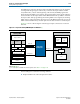


Table Of Contents
- Cyclone V Hard IP for PCI Express User Guide
- Contents
- 1. Datasheet
- 2. Getting Started with the Cyclone V Hard IP for PCI Express
- 3. Getting Started with the Avalon-MM Cyclone Hard IP for PCI Express
- Running Qsys
- Customizing the Cyclone VHard IP for PCI Express IP Core
- Adding the Remaining Components to the Qsys System
- Completing the Connections in Qsys
- Specifying Clocks and Interrupts
- Specifying Exported Interfaces
- Specifying Address Assignments
- Simulating the Example Design
- Simulating the Single DWord Design
- Understanding Channel Placement Guidelines
- Adding Synopsis Design Constraints
- Creating a Quartus II Project
- Compiling the Design
- Programming a Device
- 4. Parameter Settings for the Cyclone V Hard IP for PCI Express
- 5. Parameter Settings for the Avalon-MM Cyclone V Hard IP for PCI Express
- 6. IP Core Architecture
- Key Interfaces
- Protocol Layers
- Multi-Function Support
- PCI Express Avalon-MM Bridge
- Avalon-MM Bridge TLPs
- Avalon-MM-to-PCI Express Write Requests
- Avalon-MM-to-PCI Express Upstream Read Requests
- PCI Express-to-Avalon-MM Read Completions
- PCI Express-to-Avalon-MM Downstream Write Requests
- PCI Express-to-Avalon-MM Downstream Read Requests
- Avalon-MM-to-PCI Express Read Completions
- PCI Express-to-Avalon-MM Address Translation for Endpoints
- Minimizing BAR Sizes and the PCIe Address Space
- Avalon-MM-to-PCI Express Address Translation Algorithm
- Single DWord Completer Endpoint
- 7. IP Core Interfaces
- Cyclone V Hard IP for PCI Express
- Avalon-MM Hard IP for PCI Express
- Physical Layer Interface Signals
- Test Signals
- 8. Register Descriptions
- Configuration Space Register Content
- Altera-Defined Vendor Specific Extended Capability (VSEC)
- PCI Express Avalon-MM Bridge Control Register Access Content
- Avalon-MM to PCI Express Interrupt Registers
- PCI Express Mailbox Registers
- Avalon-MM-to-PCI Express Address Translation Table
- Root Port TLP Data Registers
- Programming Model for Avalon-MM Root Port
- PCI Express to Avalon-MM Interrupt Status and Enable Registers for Root Ports
- PCI Express to Avalon-MM Interrupt Status and Enable Registers for Endpoints
- Avalon-MM Mailbox Registers
- Correspondence between Configuration Space Registers and the PCIe Spec 2.1
- 9. Reset and Clocks
- 10. Transaction Layer Protocol (TLP) Details
- 11. Interrupts
- Interrupts for Endpoints Using the Avalon-ST Application Interface
- Interrupts for Root Ports Using the Avalon-ST Interface to the Application Layer
- Interrupts for Endpoints Using the Avalon-MM Interface to the Application Layer
- Interrupts for End Points Using the Avalon-MM Interface with Multiple MSI/MSI-X Support
- 12. Optional Features
- 13. Flow Control
- 14. Error Handling
- 15. Transceiver PHY IP Reconfiguration
- 16. SDC Timing Constraints
- 17. Testbench and Design Example
- Endpoint Testbench
- Root Port Testbench
- Chaining DMA Design Examples
- Test Driver Module
- Root Port Design Example
- Root Port BFM
- BFM Procedures and Functions
- 18. Debugging
- A. Transaction Layer Packet (TLP) Header Formats
- Additional Information

December 2013 Altera Corporation Cyclone V Hard IP for PCI Express
User Guide
17. Testbench and Design Example
This chapter introduces the Root Port or Endpoint design example including a
testbench, BFM, and a test driver module. You can create this design example using
the design described in Chapter 2, Getting Started with the Cyclone V Hard IP for PCI
Express.
When configured as an Endpoint variation, the testbench instantiates a design
example and a Root Port BFM, which provides the following functions:
■ A configuration routine that sets up all the basic configuration registers in the
Endpoint. This configuration allows the Endpoint application to be the target and
initiator of PCI Express transactions.
■ A Verilog HDL procedure interface to initiate PCI Express transactions to the
Endpoint.
The testbench uses a test driver module, altpcietb_bfm_driver_chaining to exercise
the chaining DMA of the design example. The test driver module displays
information from the Endpoint Configuration Space registers, so that you can
correlate to the parameters you specified using the parameter editor.
When configured as a Root Port, the testbench instantiates a Root Port design example
and an Endpoint model, which provides the following functions:
■ A configuration routine that sets up all the basic configuration registers in the Root
Port and the Endpoint BFM. This configuration allows the Endpoint application to
be the target and initiator of PCI Express transactions.
■ A Verilog HDL procedure interface to initiate PCI Express transactions to the
Endpoint BFM.
The testbench uses a test driver module, altpcietb_bfm_driver_rp, to exercise the
target memory and DMA channel in the Endpoint BFM. The test driver module
displays information from the Root Port Configuration Space registers, so that you
can correlate to the parameters you specified using the parameter editor. The
Endpoint model consists of an Endpoint variation combined with the chaining DMA
application described above.
1 The Altera testbench and Root Port or Endpoint BFM provide a simple method to do
basic testing of the Application Layer logic that interfaces to the variation. However,
the testbench and Root Port BFM are not intended to be a substitute for a full
verification environment. To thoroughly test your Application Layer, Altera suggests
that you obtain commercially available PCI Express verification IP and tools, or do
your own extensive hardware testing or both.
Your Application Layer design may need to handle at least the following scenarios
that are not possible to create with the Altera testbench and the Root Port BFM:
■ It is unable to generate or receive Vendor Defined Messages. Some systems
generate Vendor Defined Messages and the Application Layer must be designed
to process them. The Hard IP block passes these messages on to the Application
Layer which, in most cases should ignore them.
December 2013
UG-01110-1.5