
User guide


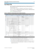
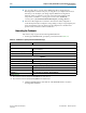
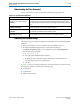

Table Of Contents
- Cyclone V Hard IP for PCI Express User Guide
- Contents
- 1. Datasheet
- 2. Getting Started with the Cyclone V Hard IP for PCI Express
- 3. Getting Started with the Avalon-MM Cyclone Hard IP for PCI Express
- Running Qsys
- Customizing the Cyclone VHard IP for PCI Express IP Core
- Adding the Remaining Components to the Qsys System
- Completing the Connections in Qsys
- Specifying Clocks and Interrupts
- Specifying Exported Interfaces
- Specifying Address Assignments
- Simulating the Example Design
- Simulating the Single DWord Design
- Understanding Channel Placement Guidelines
- Adding Synopsis Design Constraints
- Creating a Quartus II Project
- Compiling the Design
- Programming a Device
- 4. Parameter Settings for the Cyclone V Hard IP for PCI Express
- 5. Parameter Settings for the Avalon-MM Cyclone V Hard IP for PCI Express
- 6. IP Core Architecture
- Key Interfaces
- Protocol Layers
- Multi-Function Support
- PCI Express Avalon-MM Bridge
- Avalon-MM Bridge TLPs
- Avalon-MM-to-PCI Express Write Requests
- Avalon-MM-to-PCI Express Upstream Read Requests
- PCI Express-to-Avalon-MM Read Completions
- PCI Express-to-Avalon-MM Downstream Write Requests
- PCI Express-to-Avalon-MM Downstream Read Requests
- Avalon-MM-to-PCI Express Read Completions
- PCI Express-to-Avalon-MM Address Translation for Endpoints
- Minimizing BAR Sizes and the PCIe Address Space
- Avalon-MM-to-PCI Express Address Translation Algorithm
- Single DWord Completer Endpoint
- 7. IP Core Interfaces
- Cyclone V Hard IP for PCI Express
- Avalon-MM Hard IP for PCI Express
- Physical Layer Interface Signals
- Test Signals
- 8. Register Descriptions
- Configuration Space Register Content
- Altera-Defined Vendor Specific Extended Capability (VSEC)
- PCI Express Avalon-MM Bridge Control Register Access Content
- Avalon-MM to PCI Express Interrupt Registers
- PCI Express Mailbox Registers
- Avalon-MM-to-PCI Express Address Translation Table
- Root Port TLP Data Registers
- Programming Model for Avalon-MM Root Port
- PCI Express to Avalon-MM Interrupt Status and Enable Registers for Root Ports
- PCI Express to Avalon-MM Interrupt Status and Enable Registers for Endpoints
- Avalon-MM Mailbox Registers
- Correspondence between Configuration Space Registers and the PCIe Spec 2.1
- 9. Reset and Clocks
- 10. Transaction Layer Protocol (TLP) Details
- 11. Interrupts
- Interrupts for Endpoints Using the Avalon-ST Application Interface
- Interrupts for Root Ports Using the Avalon-ST Interface to the Application Layer
- Interrupts for Endpoints Using the Avalon-MM Interface to the Application Layer
- Interrupts for End Points Using the Avalon-MM Interface with Multiple MSI/MSI-X Support
- 12. Optional Features
- 13. Flow Control
- 14. Error Handling
- 15. Transceiver PHY IP Reconfiguration
- 16. SDC Timing Constraints
- 17. Testbench and Design Example
- Endpoint Testbench
- Root Port Testbench
- Chaining DMA Design Examples
- Test Driver Module
- Root Port Design Example
- Root Port BFM
- BFM Procedures and Functions
- 18. Debugging
- A. Transaction Layer Packet (TLP) Header Formats
- Additional Information

Chapter 2: Getting Started with the Cyclone V Hard IP for PCI Express 2–5
Customizing the Endpoint in the MegaWizard Plug-In Manager Design Flow
December 2013 Altera Corporation Cyclone V Hard IP for PCI Express
User Guide
10. On the Error Reporting tab, leave all options off.
11. Specify the Link settings listed in Table 2–7.
12. On the Slot Capabilities tab, leave the Slot register turned off.
13. Specify the Power Management parameters listed in Table 2–4.
14. Specify the BAR settings for Func0 listed in Table 2–5.
15. You can leave Func0 BAR3 through Func
16. 0 BAR5 and the Func0 Expansion ROM Disabled.
17. Under the Base and Limit Registers heading, disable both the Input/Output and
Prefetchable memory options. (These options are for Root Ports.)
18. For the Device ID Registers for Func0, specify the values listed in the center
column of Table 2–6. The right-hand column of this table lists the value assigned to
Altera devices. You must use the Altera values to run the reference design
described in AN 456 PCI Express High Performance Reference Design. Be sure to use
your company’s values for your final product.
Completion timeout range ABCD
Implement completion timeout disable On
Table 2–3. Link Tab
Parameter Value
Link port number 1
Slot clock configuration On
Table 2–4. Power Management Parameters
Parameter Value
Endpoint L0s acceptable exit latency Maximum of 64 ns
Endpoint L1 acceptable latency Maximum of 1 µs
Table 2–5. Base Address Registers for Func0
Parameter Value
BAR0 Type 64-bit prefetchable memory
BAR0 Size 256 MBytes - 28 bits
BAR1 Type Disabled
BAR1 Size N/A
BAR2 Type 32-bit non-prefetchable memory
BAR2 Size 1 KByte - 10 bits
Table 2–6. Device ID Registers for Func0
Register Name Value Altera Value
Vendor ID
0x00000000
0x00001172
Table 2–2. Device
Parameter Value