
User guide


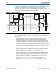

Table Of Contents
- Cyclone V Hard IP for PCI Express User Guide
- Contents
- 1. Datasheet
- 2. Getting Started with the Cyclone V Hard IP for PCI Express
- 3. Getting Started with the Avalon-MM Cyclone Hard IP for PCI Express
- Running Qsys
- Customizing the Cyclone VHard IP for PCI Express IP Core
- Adding the Remaining Components to the Qsys System
- Completing the Connections in Qsys
- Specifying Clocks and Interrupts
- Specifying Exported Interfaces
- Specifying Address Assignments
- Simulating the Example Design
- Simulating the Single DWord Design
- Understanding Channel Placement Guidelines
- Adding Synopsis Design Constraints
- Creating a Quartus II Project
- Compiling the Design
- Programming a Device
- 4. Parameter Settings for the Cyclone V Hard IP for PCI Express
- 5. Parameter Settings for the Avalon-MM Cyclone V Hard IP for PCI Express
- 6. IP Core Architecture
- Key Interfaces
- Protocol Layers
- Multi-Function Support
- PCI Express Avalon-MM Bridge
- Avalon-MM Bridge TLPs
- Avalon-MM-to-PCI Express Write Requests
- Avalon-MM-to-PCI Express Upstream Read Requests
- PCI Express-to-Avalon-MM Read Completions
- PCI Express-to-Avalon-MM Downstream Write Requests
- PCI Express-to-Avalon-MM Downstream Read Requests
- Avalon-MM-to-PCI Express Read Completions
- PCI Express-to-Avalon-MM Address Translation for Endpoints
- Minimizing BAR Sizes and the PCIe Address Space
- Avalon-MM-to-PCI Express Address Translation Algorithm
- Single DWord Completer Endpoint
- 7. IP Core Interfaces
- Cyclone V Hard IP for PCI Express
- Avalon-MM Hard IP for PCI Express
- Physical Layer Interface Signals
- Test Signals
- 8. Register Descriptions
- Configuration Space Register Content
- Altera-Defined Vendor Specific Extended Capability (VSEC)
- PCI Express Avalon-MM Bridge Control Register Access Content
- Avalon-MM to PCI Express Interrupt Registers
- PCI Express Mailbox Registers
- Avalon-MM-to-PCI Express Address Translation Table
- Root Port TLP Data Registers
- Programming Model for Avalon-MM Root Port
- PCI Express to Avalon-MM Interrupt Status and Enable Registers for Root Ports
- PCI Express to Avalon-MM Interrupt Status and Enable Registers for Endpoints
- Avalon-MM Mailbox Registers
- Correspondence between Configuration Space Registers and the PCIe Spec 2.1
- 9. Reset and Clocks
- 10. Transaction Layer Protocol (TLP) Details
- 11. Interrupts
- Interrupts for Endpoints Using the Avalon-ST Application Interface
- Interrupts for Root Ports Using the Avalon-ST Interface to the Application Layer
- Interrupts for Endpoints Using the Avalon-MM Interface to the Application Layer
- Interrupts for End Points Using the Avalon-MM Interface with Multiple MSI/MSI-X Support
- 12. Optional Features
- 13. Flow Control
- 14. Error Handling
- 15. Transceiver PHY IP Reconfiguration
- 16. SDC Timing Constraints
- 17. Testbench and Design Example
- Endpoint Testbench
- Root Port Testbench
- Chaining DMA Design Examples
- Test Driver Module
- Root Port Design Example
- Root Port BFM
- BFM Procedures and Functions
- 18. Debugging
- A. Transaction Layer Packet (TLP) Header Formats
- Additional Information
12–4 Chapter 12: Optional Features
Lane Initialization and Reversal
Cyclone V Hard IP for PCI Express December 2013 Altera Corporation
User Guide
Lane Initialization and Reversal
Connected components that include IP blocks for PCI Express need not support the
same number of lanes. The ×4 variations support initialization and operation with
components that have 1, 2, or 4 lanes.
The Cyclone V Hard IP for PCI Express supports lane reversal, which permits the
logical reversal of lane numbers for the ×1, ×2, and ×4. Lane reversal allows more
flexibility in board layout, reducing the number of signals that must cross over each
other when routing the PCB.
Table 12–3 summarizes the lane assignments for normal configuration.
Table 12–4 summarizes the lane assignments with lane reversal.
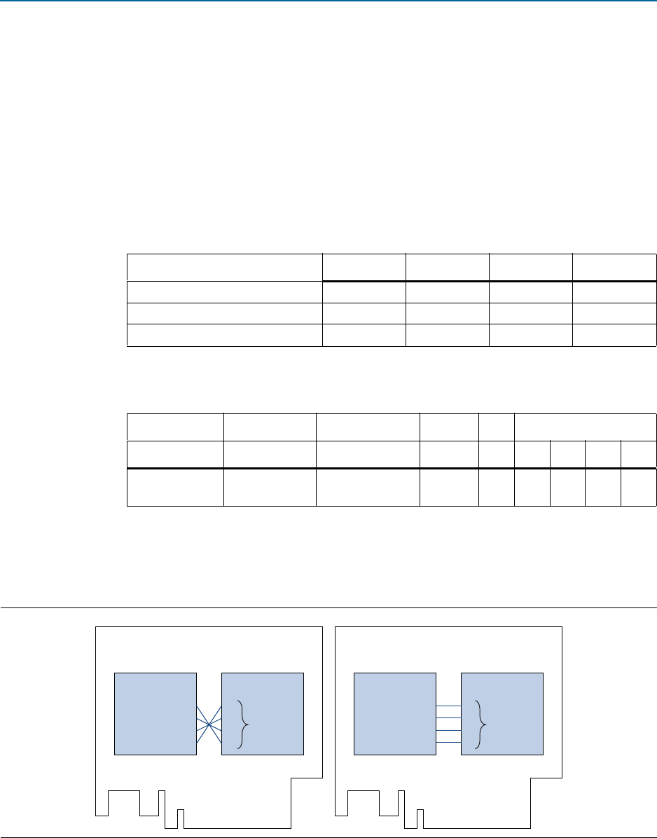
Figure 12–2 illustrates a PCI Express card with ×4 IP Root Port and a ×4 Endpoint on
the top side of the PCB. Connecting the lanes without lane reversal creates routing
problems. Using lane reversal, solves the problem.
Table 12–3. Lane Assignments without Lane Reversal
Lane Number 3 2 1 0
×4 IP core 3 2 1 0
×2 IP Core — — 1 0
×1 IP core — — — 0
Table 12–4. Lane Assignments with Lane Reversal
Core Config 4 1
Slot Size 8 4 2 18421
Lane
assignments
7:0,6:1,5:2,4:3 3:0,2:1,1:2,0:3 3:0,2:1 3:0 7:0 3:0 1:0 0:0
Figure 12–2. Using Lane Reversal to Solve PCB Routing Problems
0
1
2
3
Root Port
3
2
1
0
Endpoint
0
1
2
3
Root Port
0
1
2
3
Endpoint
No Lane Reversal
Results in PCB Routing Challenge
With Lane Reversal
Signals Route Easily
lane
reversal
no lane
reversal