
User guide

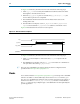
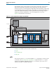


Table Of Contents
- Cyclone V Hard IP for PCI Express User Guide
- Contents
- 1. Datasheet
- 2. Getting Started with the Cyclone V Hard IP for PCI Express
- 3. Getting Started with the Avalon-MM Cyclone Hard IP for PCI Express
- Running Qsys
- Customizing the Cyclone VHard IP for PCI Express IP Core
- Adding the Remaining Components to the Qsys System
- Completing the Connections in Qsys
- Specifying Clocks and Interrupts
- Specifying Exported Interfaces
- Specifying Address Assignments
- Simulating the Example Design
- Simulating the Single DWord Design
- Understanding Channel Placement Guidelines
- Adding Synopsis Design Constraints
- Creating a Quartus II Project
- Compiling the Design
- Programming a Device
- 4. Parameter Settings for the Cyclone V Hard IP for PCI Express
- 5. Parameter Settings for the Avalon-MM Cyclone V Hard IP for PCI Express
- 6. IP Core Architecture
- Key Interfaces
- Protocol Layers
- Multi-Function Support
- PCI Express Avalon-MM Bridge
- Avalon-MM Bridge TLPs
- Avalon-MM-to-PCI Express Write Requests
- Avalon-MM-to-PCI Express Upstream Read Requests
- PCI Express-to-Avalon-MM Read Completions
- PCI Express-to-Avalon-MM Downstream Write Requests
- PCI Express-to-Avalon-MM Downstream Read Requests
- Avalon-MM-to-PCI Express Read Completions
- PCI Express-to-Avalon-MM Address Translation for Endpoints
- Minimizing BAR Sizes and the PCIe Address Space
- Avalon-MM-to-PCI Express Address Translation Algorithm
- Single DWord Completer Endpoint
- 7. IP Core Interfaces
- Cyclone V Hard IP for PCI Express
- Avalon-MM Hard IP for PCI Express
- Physical Layer Interface Signals
- Test Signals
- 8. Register Descriptions
- Configuration Space Register Content
- Altera-Defined Vendor Specific Extended Capability (VSEC)
- PCI Express Avalon-MM Bridge Control Register Access Content
- Avalon-MM to PCI Express Interrupt Registers
- PCI Express Mailbox Registers
- Avalon-MM-to-PCI Express Address Translation Table
- Root Port TLP Data Registers
- Programming Model for Avalon-MM Root Port
- PCI Express to Avalon-MM Interrupt Status and Enable Registers for Root Ports
- PCI Express to Avalon-MM Interrupt Status and Enable Registers for Endpoints
- Avalon-MM Mailbox Registers
- Correspondence between Configuration Space Registers and the PCIe Spec 2.1
- 9. Reset and Clocks
- 10. Transaction Layer Protocol (TLP) Details
- 11. Interrupts
- Interrupts for Endpoints Using the Avalon-ST Application Interface
- Interrupts for Root Ports Using the Avalon-ST Interface to the Application Layer
- Interrupts for Endpoints Using the Avalon-MM Interface to the Application Layer
- Interrupts for End Points Using the Avalon-MM Interface with Multiple MSI/MSI-X Support
- 12. Optional Features
- 13. Flow Control
- 14. Error Handling
- 15. Transceiver PHY IP Reconfiguration
- 16. SDC Timing Constraints
- 17. Testbench and Design Example
- Endpoint Testbench
- Root Port Testbench
- Chaining DMA Design Examples
- Test Driver Module
- Root Port Design Example
- Root Port BFM
- BFM Procedures and Functions
- 18. Debugging
- A. Transaction Layer Packet (TLP) Header Formats
- Additional Information
9–6 Chapter 9: Reset and Clocks
Clocks
Cyclone V Hard IP for PCI Express December 2013 Altera Corporation
User Guide
For designs that transition between Gen1 and Gen2,
pclk
can be turned off for the
entire 1 ms timeout assigned for the PHY to change the clock rate; however,
pclk
should be stable before the 1 ms timeout expires.
The CDC module implements the asynchronous clock domain crossing between the
PHY/MAC
pclk
domain and the Data Link Layer
coreclk
domain.
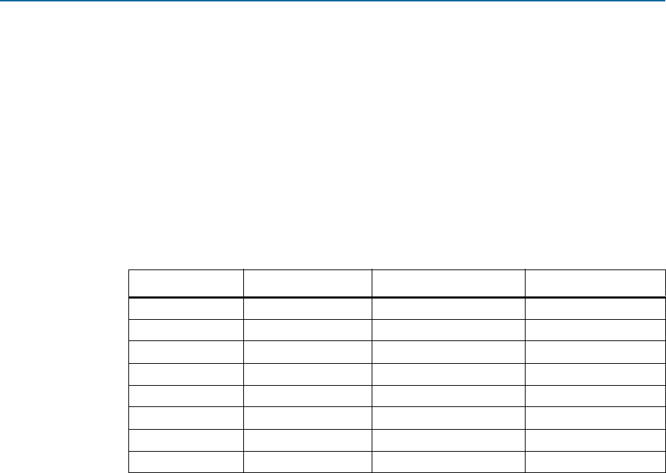
coreclkout_hip
The
coreclkout_hip
signal is derived from
pclk
. Table 9–2 lists frequencies for
coreclkout
_hip which are a function of the link width, data rate, and the width of the
Avalon-ST bus.
The frequencies and widths specified in Table 9–2 are maintained throughout
operation. If the link downtrains to a lesser link width or changes to a different
maximum link rate, it maintains the frequencies it was originally configured for as
specified in Table 9–2. (The Hard IP throttles the interface to achieve a lower
throughput.) f the link also downtrains from Gen2 to Gen1, it maintains the
frequencies from the original link width, for either Gen1 or Gen2.
pld_clk
This clock drives the Transaction Layer, Data Link Layer, part of the PHY/MAC
Layer, and the Application Layer. Ideally, the
pld_clk
drives all user logic in the
Application Layer, including other instances of the Cyclone V Hard IP for PCI Express
and memory interfaces. Using a single clock simplifies timing. You should derive the
pld_clk
clock from the
coreclkout_hip
output clock pin.
pld_clk
does not have to be
phase locked to
coreclkout_hip
because the clock domain crossing logic handles this
timing issue.
Transceiver Clock Signals
As Figure 9–5 indicates, there are two clock inputs to the PHY IP Core for PCI Express
IP core transceiver.
■
refclk
—You must provide this 100 MHz or 125 MHz reference clock to the
Cyclone V Hard IP for PCI Express IP core.
Table 9–2. coreclkout_hip Values for All Parameterizations
Link Width Max Link Rate Avalon Interface Width coreclkout_hip
×1 Gen1 64 125 MHz
×1 Gen1 64 62.5 MHz
(1)
×2 Gen1 64 125 MHz
×4 Gen1 64 125 MHz
×1 Gen2 64 62.5 MHz
(1)
×1 Gen2 64 125 MHz
×2 Gen2 64 125 MHz
×4 Gen2 128 125 MHz
Note to Table 9–2:
(1) This mode saves power.