
User guide
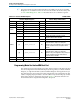
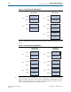
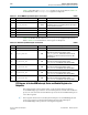
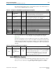
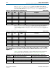


Table Of Contents
- Cyclone V Hard IP for PCI Express User Guide
- Contents
- 1. Datasheet
- 2. Getting Started with the Cyclone V Hard IP for PCI Express
- 3. Getting Started with the Avalon-MM Cyclone Hard IP for PCI Express
- Running Qsys
- Customizing the Cyclone VHard IP for PCI Express IP Core
- Adding the Remaining Components to the Qsys System
- Completing the Connections in Qsys
- Specifying Clocks and Interrupts
- Specifying Exported Interfaces
- Specifying Address Assignments
- Simulating the Example Design
- Simulating the Single DWord Design
- Understanding Channel Placement Guidelines
- Adding Synopsis Design Constraints
- Creating a Quartus II Project
- Compiling the Design
- Programming a Device
- 4. Parameter Settings for the Cyclone V Hard IP for PCI Express
- 5. Parameter Settings for the Avalon-MM Cyclone V Hard IP for PCI Express
- 6. IP Core Architecture
- Key Interfaces
- Protocol Layers
- Multi-Function Support
- PCI Express Avalon-MM Bridge
- Avalon-MM Bridge TLPs
- Avalon-MM-to-PCI Express Write Requests
- Avalon-MM-to-PCI Express Upstream Read Requests
- PCI Express-to-Avalon-MM Read Completions
- PCI Express-to-Avalon-MM Downstream Write Requests
- PCI Express-to-Avalon-MM Downstream Read Requests
- Avalon-MM-to-PCI Express Read Completions
- PCI Express-to-Avalon-MM Address Translation for Endpoints
- Minimizing BAR Sizes and the PCIe Address Space
- Avalon-MM-to-PCI Express Address Translation Algorithm
- Single DWord Completer Endpoint
- 7. IP Core Interfaces
- Cyclone V Hard IP for PCI Express
- Avalon-MM Hard IP for PCI Express
- Physical Layer Interface Signals
- Test Signals
- 8. Register Descriptions
- Configuration Space Register Content
- Altera-Defined Vendor Specific Extended Capability (VSEC)
- PCI Express Avalon-MM Bridge Control Register Access Content
- Avalon-MM to PCI Express Interrupt Registers
- PCI Express Mailbox Registers
- Avalon-MM-to-PCI Express Address Translation Table
- Root Port TLP Data Registers
- Programming Model for Avalon-MM Root Port
- PCI Express to Avalon-MM Interrupt Status and Enable Registers for Root Ports
- PCI Express to Avalon-MM Interrupt Status and Enable Registers for Endpoints
- Avalon-MM Mailbox Registers
- Correspondence between Configuration Space Registers and the PCIe Spec 2.1
- 9. Reset and Clocks
- 10. Transaction Layer Protocol (TLP) Details
- 11. Interrupts
- Interrupts for Endpoints Using the Avalon-ST Application Interface
- Interrupts for Root Ports Using the Avalon-ST Interface to the Application Layer
- Interrupts for Endpoints Using the Avalon-MM Interface to the Application Layer
- Interrupts for End Points Using the Avalon-MM Interface with Multiple MSI/MSI-X Support
- 12. Optional Features
- 13. Flow Control
- 14. Error Handling
- 15. Transceiver PHY IP Reconfiguration
- 16. SDC Timing Constraints
- 17. Testbench and Design Example
- Endpoint Testbench
- Root Port Testbench
- Chaining DMA Design Examples
- Test Driver Module
- Root Port Design Example
- Root Port BFM
- BFM Procedures and Functions
- 18. Debugging
- A. Transaction Layer Packet (TLP) Header Formats
- Additional Information

8–22 Chapter 8: Register Descriptions
Correspondence between Configuration Space Registers and the PCIe Spec 2.1
Cyclone V Hard IP for PCI Express December 2013 Altera Corporation
User Guide
The
Avalon-MM-to-PCI Express Mailbox
registers are writable at the addresses
shown in Table 8–37. When the Avalon-MM processor writes to one of these registers
the corresponding bit in the
PCI Express Interrupt Status
register is set to 1.
The
PCI Express-to-Avalon-MM Mailbox
registers are read-only at the addresses
shown in Table 8–38. The Avalon-MM processor reads these registers when the
corresponding bit in the
PCI Express to Avalon-MM Interrupt Status
register is set
to 1.
Correspondence between Configuration Space Registers and the PCIe
Spec 2.1
Table 8–39 provides a comprehensive correspondence between the Configuration
Space registers and their descriptions in the PCI Express Base Specification 2.1.
Table 8–37. Avalon-MM-to-PCI Express Mailbox Registers 0x3A00–0x3A1F
Address Name Access Description
0x3A00 A2P_MAILBOX0 RW Avalon-MM-to-PCI Express mailbox 0
0x3A04 A2P_MAILBOX1 RW Avalon-MM-to-PCI Express mailbox 1
0x3A08 A2P _MAILBOX2 RW Avalon-MM-to-PCI Express mailbox 2
0x3A0C A2P _MAILBOX3 RW Avalon-MM-to-PCI Express mailbox 3
0x3A10 A2P _MAILBOX4 RW Avalon-MM-to-PCI Express mailbox 4
0x3A14 A2P _MAILBOX5 RW Avalon-MM-to-PCI Express mailbox 5
0x3A18 A2P _MAILBOX6 RW Avalon-MM-to-PCI Express mailbox 6
0x3A1C A2P_MAILBOX7 RW Avalon-MM-to-PCI Express mailbox 7
Table 8–38. PCI Express-to-Avalon-MM Mailbox Registers 0x3B00–0x3B1F
Address Name
Access
Mode
Description
0x3B00 P2A_MAILBOX0 RO PCI Express-to-Avalon-MM mailbox 0.
0x3B04 P2A_MAILBOX1 RO PCI Express-to-Avalon-MM mailbox 1
0x3B08 P2A_MAILBOX2 RO PCI Express-to-Avalon-MM mailbox 2
0x3B0C P2A_MAILBOX3 RO PCI Express-to-Avalon-MM mailbox 3
0x3B10 P2A_MAILBOX4 RO PCI Express-to-Avalon-MM mailbox 4
0x3B14 P2A_MAILBOX5 RO PCI Express-to-Avalon-MM mailbox 5
0x3B18 P2A_MAILBOX6 RO PCI Express-to-Avalon-MM mailbox 6
0x3B1C P2A_MAILBOX7 RO PCI Express-to-Avalon-MM mailbox 7
Table 8–39. Correspondence Configuration Space Registers and PCIe Base Specification Rev. 2.1 (Part 1 of 4)
Byte Address Hard IP Configuration Space Register Corresponding Section in PCIe Specification
Table 6-1. Common Configuration Space Header
0x000:0x03C PCI Header Type 0 Configuration Registers Type 0 Configuration Space Header
0x000:0x03C PCI Header Type 1 Configuration Registers Type 1 Configuration Space Header
0x040:0x04C Reserved