
User guide
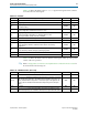
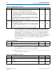
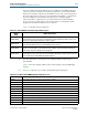
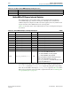

Table Of Contents
- Cyclone V Hard IP for PCI Express User Guide
- Contents
- 1. Datasheet
- 2. Getting Started with the Cyclone V Hard IP for PCI Express
- 3. Getting Started with the Avalon-MM Cyclone Hard IP for PCI Express
- Running Qsys
- Customizing the Cyclone VHard IP for PCI Express IP Core
- Adding the Remaining Components to the Qsys System
- Completing the Connections in Qsys
- Specifying Clocks and Interrupts
- Specifying Exported Interfaces
- Specifying Address Assignments
- Simulating the Example Design
- Simulating the Single DWord Design
- Understanding Channel Placement Guidelines
- Adding Synopsis Design Constraints
- Creating a Quartus II Project
- Compiling the Design
- Programming a Device
- 4. Parameter Settings for the Cyclone V Hard IP for PCI Express
- 5. Parameter Settings for the Avalon-MM Cyclone V Hard IP for PCI Express
- 6. IP Core Architecture
- Key Interfaces
- Protocol Layers
- Multi-Function Support
- PCI Express Avalon-MM Bridge
- Avalon-MM Bridge TLPs
- Avalon-MM-to-PCI Express Write Requests
- Avalon-MM-to-PCI Express Upstream Read Requests
- PCI Express-to-Avalon-MM Read Completions
- PCI Express-to-Avalon-MM Downstream Write Requests
- PCI Express-to-Avalon-MM Downstream Read Requests
- Avalon-MM-to-PCI Express Read Completions
- PCI Express-to-Avalon-MM Address Translation for Endpoints
- Minimizing BAR Sizes and the PCIe Address Space
- Avalon-MM-to-PCI Express Address Translation Algorithm
- Single DWord Completer Endpoint
- 7. IP Core Interfaces
- Cyclone V Hard IP for PCI Express
- Avalon-MM Hard IP for PCI Express
- Physical Layer Interface Signals
- Test Signals
- 8. Register Descriptions
- Configuration Space Register Content
- Altera-Defined Vendor Specific Extended Capability (VSEC)
- PCI Express Avalon-MM Bridge Control Register Access Content
- Avalon-MM to PCI Express Interrupt Registers
- PCI Express Mailbox Registers
- Avalon-MM-to-PCI Express Address Translation Table
- Root Port TLP Data Registers
- Programming Model for Avalon-MM Root Port
- PCI Express to Avalon-MM Interrupt Status and Enable Registers for Root Ports
- PCI Express to Avalon-MM Interrupt Status and Enable Registers for Endpoints
- Avalon-MM Mailbox Registers
- Correspondence between Configuration Space Registers and the PCIe Spec 2.1
- 9. Reset and Clocks
- 10. Transaction Layer Protocol (TLP) Details
- 11. Interrupts
- Interrupts for Endpoints Using the Avalon-ST Application Interface
- Interrupts for Root Ports Using the Avalon-ST Interface to the Application Layer
- Interrupts for Endpoints Using the Avalon-MM Interface to the Application Layer
- Interrupts for End Points Using the Avalon-MM Interface with Multiple MSI/MSI-X Support
- 12. Optional Features
- 13. Flow Control
- 14. Error Handling
- 15. Transceiver PHY IP Reconfiguration
- 16. SDC Timing Constraints
- 17. Testbench and Design Example
- Endpoint Testbench
- Root Port Testbench
- Chaining DMA Design Examples
- Test Driver Module
- Root Port Design Example
- Root Port BFM
- BFM Procedures and Functions
- 18. Debugging
- A. Transaction Layer Packet (TLP) Header Formats
- Additional Information
8–14 Chapter 8: Register Descriptions
PCI Express Avalon-MM Bridge Control Register Access Content
Cyclone V Hard IP for PCI Express December 2013 Altera Corporation
User Guide
The Avalon-MM-to-PCI Express Mailbox registers are read at the addresses shown in
Table 8–29. The PCI Express Root Complex should use these addresses to read the
mailbox information after being signaled by the corresponding bits in the PCI Express
Interrupt Status
register.
Avalon-MM-to-PCI Express Address Translation Table
The Avalon-MM-to-PCI Express address translation table is writable using the CRA
slave port. Each entry in the PCI Express address translation table (Table 8–30) is 8
bytes wide, regardless of the value in the current PCI Express address width
parameter. Therefore, register addresses are always the same width, regardless of PCI
Express address width.
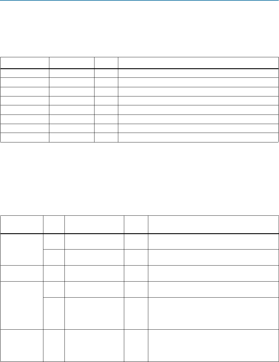
Table 8–29. Avalon-MM-to-PCI Express Mailbox Registers 0x0900–0x091F
Address Name Access Description
0x0900 A2P_MAILBOX0 RO Avalon-MM-to-PCI Express Mailbox 0
0x0904 A2P_MAILBOX1 RO Avalon-MM-to-PCI Express Mailbox 1
0x0908 A2P_MAILBOX2 RO Avalon-MM-to-PCI Express Mailbox 2
0x090C A2P_MAILBOX3 RO Avalon-MM-to-PCI Express Mailbox 3
0x0910 A2P_MAILBOX4 RO Avalon-MM-to-PCI Express Mailbox 4
0x0914 A2P_MAILBOX5 RO Avalon-MM-to-PCI Express Mailbox 5
0x0918 A2P_MAILBOX6 RO Avalon-MM-to-PCI Express Mailbox 6
0x091C A2P_MAILBOX7 RO Avalon-MM-to-PCI Express Mailbox 7
Table 8–30. Avalon-MM-to-PCI Express Address Translation Table 0x1000–0x1FFF
Address Bits Name
Access
Description
0x1000
[1:0] A2P_ADDR_SPACE0 RW
Address space indication for entry 0. Refer to Table 8–31
for the definition of these bits.
[31:2] A2P_ADDR_MAP_LO0 RW
Lower bits of Avalon-MM-to-PCI Express address map
entry 0.
0x1004 [31:0] A2P_ADDR_MAP_HI0 RW
Upper bits of Avalon-MM-to-PCI Express address map
entry 0.
0x1008
[1:0] A2P_ADDR_SPACE1 RW
Address space indication for entry 1. Refer to Table 8–31
for the definition of these bits.
[31:2] A2P_ADDR_MAP_LO1 RW
Lower bits of Avalon-MM-to-PCI Express address map
entry 1.
This entry is only implemented if number of address
translation table entries is greater than 1.
0x100C [31:0] A2P_ADDR_MAP_HI1 RW
Upper bits of Avalon-MM-to-PCI Express address map
entry 1.
This entry is only implemented if the number of address
translations table entries is greater than 1.
Note to Table 8–30:
(1) These table entries are repeated for each address specified in the Number of address pages parameter. If Number of address pages is set to
the maximum of 512, 0x1FF8 contains A2P_ADDR_MAP_LO511 and 0x1FFC contains A2P_ADDR_MAP_HI511.