
User guide
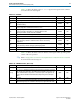
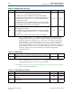
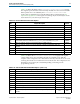
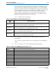
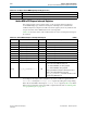
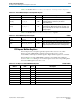
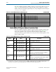

Table Of Contents
- Cyclone V Hard IP for PCI Express User Guide
- Contents
- 1. Datasheet
- 2. Getting Started with the Cyclone V Hard IP for PCI Express
- 3. Getting Started with the Avalon-MM Cyclone Hard IP for PCI Express
- Running Qsys
- Customizing the Cyclone VHard IP for PCI Express IP Core
- Adding the Remaining Components to the Qsys System
- Completing the Connections in Qsys
- Specifying Clocks and Interrupts
- Specifying Exported Interfaces
- Specifying Address Assignments
- Simulating the Example Design
- Simulating the Single DWord Design
- Understanding Channel Placement Guidelines
- Adding Synopsis Design Constraints
- Creating a Quartus II Project
- Compiling the Design
- Programming a Device
- 4. Parameter Settings for the Cyclone V Hard IP for PCI Express
- 5. Parameter Settings for the Avalon-MM Cyclone V Hard IP for PCI Express
- 6. IP Core Architecture
- Key Interfaces
- Protocol Layers
- Multi-Function Support
- PCI Express Avalon-MM Bridge
- Avalon-MM Bridge TLPs
- Avalon-MM-to-PCI Express Write Requests
- Avalon-MM-to-PCI Express Upstream Read Requests
- PCI Express-to-Avalon-MM Read Completions
- PCI Express-to-Avalon-MM Downstream Write Requests
- PCI Express-to-Avalon-MM Downstream Read Requests
- Avalon-MM-to-PCI Express Read Completions
- PCI Express-to-Avalon-MM Address Translation for Endpoints
- Minimizing BAR Sizes and the PCIe Address Space
- Avalon-MM-to-PCI Express Address Translation Algorithm
- Single DWord Completer Endpoint
- 7. IP Core Interfaces
- Cyclone V Hard IP for PCI Express
- Avalon-MM Hard IP for PCI Express
- Physical Layer Interface Signals
- Test Signals
- 8. Register Descriptions
- Configuration Space Register Content
- Altera-Defined Vendor Specific Extended Capability (VSEC)
- PCI Express Avalon-MM Bridge Control Register Access Content
- Avalon-MM to PCI Express Interrupt Registers
- PCI Express Mailbox Registers
- Avalon-MM-to-PCI Express Address Translation Table
- Root Port TLP Data Registers
- Programming Model for Avalon-MM Root Port
- PCI Express to Avalon-MM Interrupt Status and Enable Registers for Root Ports
- PCI Express to Avalon-MM Interrupt Status and Enable Registers for Endpoints
- Avalon-MM Mailbox Registers
- Correspondence between Configuration Space Registers and the PCIe Spec 2.1
- 9. Reset and Clocks
- 10. Transaction Layer Protocol (TLP) Details
- 11. Interrupts
- Interrupts for Endpoints Using the Avalon-ST Application Interface
- Interrupts for Root Ports Using the Avalon-ST Interface to the Application Layer
- Interrupts for Endpoints Using the Avalon-MM Interface to the Application Layer
- Interrupts for End Points Using the Avalon-MM Interface with Multiple MSI/MSI-X Support
- 12. Optional Features
- 13. Flow Control
- 14. Error Handling
- 15. Transceiver PHY IP Reconfiguration
- 16. SDC Timing Constraints
- 17. Testbench and Design Example
- Endpoint Testbench
- Root Port Testbench
- Chaining DMA Design Examples
- Test Driver Module
- Root Port Design Example
- Root Port BFM
- BFM Procedures and Functions
- 18. Debugging
- A. Transaction Layer Packet (TLP) Header Formats
- Additional Information

Chapter 8: Register Descriptions 8–11
PCI Express Avalon-MM Bridge Control Register Access Content
December 2013 Altera Corporation Cyclone V Hard IP for PCI Express
User Guide
The control and status register address space is 16 KBytes. Each 4 KByte sub-region
contains a specific set of functions, which may be specific to accesses from the PCI
Express Root Complex only, from Avalon-MM processors only, or from both types of
processors. Because all accesses come across the interconnect fabric —requests from
the Avalon-MM Cyclone V Hard IP for PCI Express are routed through the
interconnect fabric— hardware does not enforce restrictions to limit individual
processor access to specific regions. However, the regions are designed to enable
straight-forward enforcement by processor software.
Table 8–23 describes the four subregions.
1 The data returned for a read issued to any undefined address in this range is
unpredictable.
Table 8–24 lists the complete address map for the PCI Express Avalon-MM bridge
registers.
1 In Table 8–24 the text in green links to the detailed register description.
Table 8–23. Avalon-MM Control and Status Register Address Spaces
Address
Range
Address Space Usage
0x0000-0x0FFF
Registers typically intended for access by PCI Express processors only. This includes PCI Express
interrupt enable controls, write access to the PCI Express Avalon-MM bridge mailbox registers, and
read access to Avalon-MM-to-PCI Express mailbox registers.
0x1000-0x1FFF
Avalon-MM-to-PCI Express address translation tables. Depending on the system design these may be
accessed by PCI Express processors, Avalon-MM processors, or both.
0x2000-0x2FFF
Root Port request registers. An embedded processor, such as the Nios II processor, programs these
registers to send the data to send Configuration TLPs, I/O TLPs, single dword Memory Reads and
Write request, and receive interrupts from an Endpoint.
0x3000-0x3FFF
Registers typically intended for access by Avalon-MM processors only. These include Avalon-MM
interrupt enable controls, write access to the Avalon-MM-to-PCI Express mailbox registers, and read
access to PCI Express Avalon-MM bridge mailbox registers.
Table 8–24. PCI Express Avalon-MM Bridge Register Map (Part 1 of 2)
Address Range Register
0x0040 Avalon-MM to PCI Express Interrupt Status Register 0x0040
0x0050 Avalon-MM to PCI Express Interrupt Enable Register 0x0050
0x0060 Avalon-MM Interrupt Vector Register 0x0060
0x0800-0x081F PCI Express-to-Avalon-MM Mailbox Registers 0x0800–0x081F
0x0900-0x091F Avalon-MM-to-PCI Express Mailbox Registers 0x0900–0x091F
0x1000-0x1FFF Avalon-MM-to-PCI Express Address Translation Table 0x1000–0x1FFF
0x2000–0x2FFF Root Port TLP Data Registers 0x2000–0x2FFF
0x3060 Avalon-MM Interrupt Status Registers for Root Ports 0x3060
0x3060 PCI Express to Avalon-MM Interrupt Status Register for Endpoints 0x3060
0x3070 INT-X Interrupt Enable Register for Root Ports 0x3070
0x3070 INT-X Interrupt Enable Register for Endpoints 0x3070