
User guide
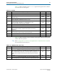
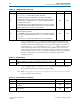
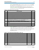
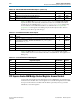
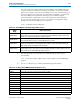
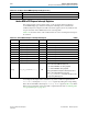
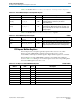
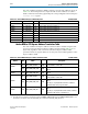

Table Of Contents
- Cyclone V Hard IP for PCI Express User Guide
- Contents
- 1. Datasheet
- 2. Getting Started with the Cyclone V Hard IP for PCI Express
- 3. Getting Started with the Avalon-MM Cyclone Hard IP for PCI Express
- Running Qsys
- Customizing the Cyclone VHard IP for PCI Express IP Core
- Adding the Remaining Components to the Qsys System
- Completing the Connections in Qsys
- Specifying Clocks and Interrupts
- Specifying Exported Interfaces
- Specifying Address Assignments
- Simulating the Example Design
- Simulating the Single DWord Design
- Understanding Channel Placement Guidelines
- Adding Synopsis Design Constraints
- Creating a Quartus II Project
- Compiling the Design
- Programming a Device
- 4. Parameter Settings for the Cyclone V Hard IP for PCI Express
- 5. Parameter Settings for the Avalon-MM Cyclone V Hard IP for PCI Express
- 6. IP Core Architecture
- Key Interfaces
- Protocol Layers
- Multi-Function Support
- PCI Express Avalon-MM Bridge
- Avalon-MM Bridge TLPs
- Avalon-MM-to-PCI Express Write Requests
- Avalon-MM-to-PCI Express Upstream Read Requests
- PCI Express-to-Avalon-MM Read Completions
- PCI Express-to-Avalon-MM Downstream Write Requests
- PCI Express-to-Avalon-MM Downstream Read Requests
- Avalon-MM-to-PCI Express Read Completions
- PCI Express-to-Avalon-MM Address Translation for Endpoints
- Minimizing BAR Sizes and the PCIe Address Space
- Avalon-MM-to-PCI Express Address Translation Algorithm
- Single DWord Completer Endpoint
- 7. IP Core Interfaces
- Cyclone V Hard IP for PCI Express
- Avalon-MM Hard IP for PCI Express
- Physical Layer Interface Signals
- Test Signals
- 8. Register Descriptions
- Configuration Space Register Content
- Altera-Defined Vendor Specific Extended Capability (VSEC)
- PCI Express Avalon-MM Bridge Control Register Access Content
- Avalon-MM to PCI Express Interrupt Registers
- PCI Express Mailbox Registers
- Avalon-MM-to-PCI Express Address Translation Table
- Root Port TLP Data Registers
- Programming Model for Avalon-MM Root Port
- PCI Express to Avalon-MM Interrupt Status and Enable Registers for Root Ports
- PCI Express to Avalon-MM Interrupt Status and Enable Registers for Endpoints
- Avalon-MM Mailbox Registers
- Correspondence between Configuration Space Registers and the PCIe Spec 2.1
- 9. Reset and Clocks
- 10. Transaction Layer Protocol (TLP) Details
- 11. Interrupts
- Interrupts for Endpoints Using the Avalon-ST Application Interface
- Interrupts for Root Ports Using the Avalon-ST Interface to the Application Layer
- Interrupts for Endpoints Using the Avalon-MM Interface to the Application Layer
- Interrupts for End Points Using the Avalon-MM Interface with Multiple MSI/MSI-X Support
- 12. Optional Features
- 13. Flow Control
- 14. Error Handling
- 15. Transceiver PHY IP Reconfiguration
- 16. SDC Timing Constraints
- 17. Testbench and Design Example
- Endpoint Testbench
- Root Port Testbench
- Chaining DMA Design Examples
- Test Driver Module
- Root Port Design Example
- Root Port BFM
- BFM Procedures and Functions
- 18. Debugging
- A. Transaction Layer Packet (TLP) Header Formats
- Additional Information
8–10 Chapter 8: Register Descriptions
PCI Express Avalon-MM Bridge Control Register Access Content
Cyclone V Hard IP for PCI Express December 2013 Altera Corporation
User Guide
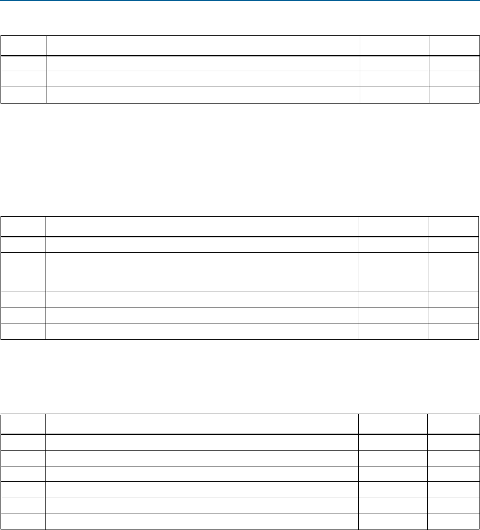
Table 8–21 defines the
Correctable Internal Error Status
register. This register
reports the status of the internally checked errors that are correctable. When these
specific errors are enabled by the
Correctable Internal Error Mask
register, they
are forwarded as Correctable Internal Errors as defined in the PCI Express Base
Specification 3.0. This register is for debug only. It should only be used to observe
behavior, not to drive logic custom logic.
Table 8–22 defines the
Correctable Internal Error Mask
register. This register
controls which errors are forwarded as Internal Correctable Errors. This register is for
debug only.
S
PCI Express Avalon-MM Bridge Control Register Access Content
Control and status registers in the PCI Express Avalon-MM bridge are implemented
in the CRA slave module. The control registers are accessible through the Avalon-MM
slave port of the CRA slave module. This module is optional; however, you must
include it to access the registers.
[2] Mask for data parity error detected at the input to the RX Buffer. 1b’1 RWS
[1] Mask for the retry buffer uncorrectable ECC error. 1b’1 RWS
[0] Mask for the RX buffer uncorrectable ECC error. 1b’1 RWS
Table 8–20. Uncorrectable Internal Error Mask Register (Part 2 of 2)
Bits Register Description Reset Value Access
Table 8–21. Correctable Internal Error Status Register
Bits Register Description Reset Value Access
[31:6] Reserved. 0 RO
[5]
When set, indicates a configuration error has been detected in CvP mode which
is reported as correctable. This bit is set whenever a
CVP_CONFIG_ERROR
occurs while in
CVP_MODE
.
0RW1CS
[4:2] Reserved. 0 RO
[1] When set, the retry buffer correctable ECC error status indicates an error. 0 RW1CS
[0] When set, the RX buffer correctable ECC error status indicates an error. 0 RW1CS
Table 8–22. Correctable Internal Error Mask Register
Bits Register Description Reset Value Access
[31:7] Reserved. 0 RO
[6] Mask for Corrected Internal Error reported by the Application Layer. 1 RWS
[5] Mask for configuration error detected in CvP mode. 0 RWS
[4:2] Reserved. 0 RO
[1] Mask for retry buffer correctable ECC error. 1 RWS
[0] Mask for RX Buffer correctable ECC error. 1 RWS