
User guide
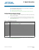
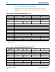
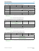
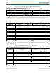
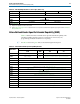
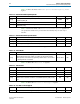
Table Of Contents
- Cyclone V Hard IP for PCI Express User Guide
- Contents
- 1. Datasheet
- 2. Getting Started with the Cyclone V Hard IP for PCI Express
- 3. Getting Started with the Avalon-MM Cyclone Hard IP for PCI Express
- Running Qsys
- Customizing the Cyclone VHard IP for PCI Express IP Core
- Adding the Remaining Components to the Qsys System
- Completing the Connections in Qsys
- Specifying Clocks and Interrupts
- Specifying Exported Interfaces
- Specifying Address Assignments
- Simulating the Example Design
- Simulating the Single DWord Design
- Understanding Channel Placement Guidelines
- Adding Synopsis Design Constraints
- Creating a Quartus II Project
- Compiling the Design
- Programming a Device
- 4. Parameter Settings for the Cyclone V Hard IP for PCI Express
- 5. Parameter Settings for the Avalon-MM Cyclone V Hard IP for PCI Express
- 6. IP Core Architecture
- Key Interfaces
- Protocol Layers
- Multi-Function Support
- PCI Express Avalon-MM Bridge
- Avalon-MM Bridge TLPs
- Avalon-MM-to-PCI Express Write Requests
- Avalon-MM-to-PCI Express Upstream Read Requests
- PCI Express-to-Avalon-MM Read Completions
- PCI Express-to-Avalon-MM Downstream Write Requests
- PCI Express-to-Avalon-MM Downstream Read Requests
- Avalon-MM-to-PCI Express Read Completions
- PCI Express-to-Avalon-MM Address Translation for Endpoints
- Minimizing BAR Sizes and the PCIe Address Space
- Avalon-MM-to-PCI Express Address Translation Algorithm
- Single DWord Completer Endpoint
- 7. IP Core Interfaces
- Cyclone V Hard IP for PCI Express
- Avalon-MM Hard IP for PCI Express
- Physical Layer Interface Signals
- Test Signals
- 8. Register Descriptions
- Configuration Space Register Content
- Altera-Defined Vendor Specific Extended Capability (VSEC)
- PCI Express Avalon-MM Bridge Control Register Access Content
- Avalon-MM to PCI Express Interrupt Registers
- PCI Express Mailbox Registers
- Avalon-MM-to-PCI Express Address Translation Table
- Root Port TLP Data Registers
- Programming Model for Avalon-MM Root Port
- PCI Express to Avalon-MM Interrupt Status and Enable Registers for Root Ports
- PCI Express to Avalon-MM Interrupt Status and Enable Registers for Endpoints
- Avalon-MM Mailbox Registers
- Correspondence between Configuration Space Registers and the PCIe Spec 2.1
- 9. Reset and Clocks
- 10. Transaction Layer Protocol (TLP) Details
- 11. Interrupts
- Interrupts for Endpoints Using the Avalon-ST Application Interface
- Interrupts for Root Ports Using the Avalon-ST Interface to the Application Layer
- Interrupts for Endpoints Using the Avalon-MM Interface to the Application Layer
- Interrupts for End Points Using the Avalon-MM Interface with Multiple MSI/MSI-X Support
- 12. Optional Features
- 13. Flow Control
- 14. Error Handling
- 15. Transceiver PHY IP Reconfiguration
- 16. SDC Timing Constraints
- 17. Testbench and Design Example
- Endpoint Testbench
- Root Port Testbench
- Chaining DMA Design Examples
- Test Driver Module
- Root Port Design Example
- Root Port BFM
- BFM Procedures and Functions
- 18. Debugging
- A. Transaction Layer Packet (TLP) Header Formats
- Additional Information

8–6 Chapter 8: Register Descriptions
Altera-Defined Vendor Specific Extended Capability (VSEC)
Cyclone V Hard IP for PCI Express December 2013 Altera Corporation
User Guide
Table 8–10 defines the fields of the
Vendor Specific Extended Capability Header
register.
Table 8–11 defines the fields of the
Altera-Defined Vendor Specific
register. You
can specify these fields when you instantiate the Hard IP; they are read-only at
run-time.
Table 8–12 defines the
Altera Marker
register.
Table 8–13 defines the
JTAG Silicon ID
registers.
Table 8–14 defines the
User Device or Board Type ID
register.
Table 8–10. Altera-Defined VSEC Capability Header
Bits Register Description Value Access
[15:0]
PCI Express Extended Capability ID
. PCIe specification defined value
for VSEC Capability ID.
0x000B RO
[19:16]
Version
. PCIe specification defined value for VSEC version. 0x1 RO
[31:20]
Next Capability Offset
. Starting address of the next Capability Structure
implemented, if any.
Variable RO
Table 8–11. Altera-Defined Vendor Specific Header
Bits Register Description Value Access
[15:0]
VSEC ID
. A user configurable VSEC ID. User entered RO
[19:16]
VSEC Revision
. A user configurable VSEC revision. Variable RO
[31:20]
VSEC Length
. Total length of this structure in bytes. 0x044 RO
Table 8–12. Altera Marker
Bits Register Description Value Access
[31:0]
Altera Marker
. This read only register is an additional marker. If you use the
standard Altera Programmer software to configure the device with CvP, this
marker provides a value that the programming software reads to ensure that it
is operating with the correct VSEC.
A Device Value RO
Table 8–13. JTAG Silicon ID
Bits Register Description Value Access
[127:96]
JTAG Silicon ID DW3
TBD RO
[95:64]
JTAG Silicon ID DW2
TBD RO
[63:32]
JTAG Silicon ID DW1
TBD RO
[31:0]
JTAG Silicon ID DW0
- This is the JTAG Silicon ID that CvP programming
software reads to determine to that the correct SRAM object file (.sof) is being
used.
TBD RO
Table 8–14. User Device or Board Type ID
Bits Register Description Value Access
[15:0] Configurable device or board type ID to specify to CvP the correct .sof. Variable RO