
User guide

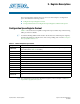
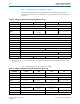
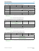
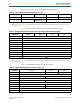
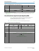
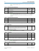
Table Of Contents
- Cyclone V Hard IP for PCI Express User Guide
- Contents
- 1. Datasheet
- 2. Getting Started with the Cyclone V Hard IP for PCI Express
- 3. Getting Started with the Avalon-MM Cyclone Hard IP for PCI Express
- Running Qsys
- Customizing the Cyclone VHard IP for PCI Express IP Core
- Adding the Remaining Components to the Qsys System
- Completing the Connections in Qsys
- Specifying Clocks and Interrupts
- Specifying Exported Interfaces
- Specifying Address Assignments
- Simulating the Example Design
- Simulating the Single DWord Design
- Understanding Channel Placement Guidelines
- Adding Synopsis Design Constraints
- Creating a Quartus II Project
- Compiling the Design
- Programming a Device
- 4. Parameter Settings for the Cyclone V Hard IP for PCI Express
- 5. Parameter Settings for the Avalon-MM Cyclone V Hard IP for PCI Express
- 6. IP Core Architecture
- Key Interfaces
- Protocol Layers
- Multi-Function Support
- PCI Express Avalon-MM Bridge
- Avalon-MM Bridge TLPs
- Avalon-MM-to-PCI Express Write Requests
- Avalon-MM-to-PCI Express Upstream Read Requests
- PCI Express-to-Avalon-MM Read Completions
- PCI Express-to-Avalon-MM Downstream Write Requests
- PCI Express-to-Avalon-MM Downstream Read Requests
- Avalon-MM-to-PCI Express Read Completions
- PCI Express-to-Avalon-MM Address Translation for Endpoints
- Minimizing BAR Sizes and the PCIe Address Space
- Avalon-MM-to-PCI Express Address Translation Algorithm
- Single DWord Completer Endpoint
- 7. IP Core Interfaces
- Cyclone V Hard IP for PCI Express
- Avalon-MM Hard IP for PCI Express
- Physical Layer Interface Signals
- Test Signals
- 8. Register Descriptions
- Configuration Space Register Content
- Altera-Defined Vendor Specific Extended Capability (VSEC)
- PCI Express Avalon-MM Bridge Control Register Access Content
- Avalon-MM to PCI Express Interrupt Registers
- PCI Express Mailbox Registers
- Avalon-MM-to-PCI Express Address Translation Table
- Root Port TLP Data Registers
- Programming Model for Avalon-MM Root Port
- PCI Express to Avalon-MM Interrupt Status and Enable Registers for Root Ports
- PCI Express to Avalon-MM Interrupt Status and Enable Registers for Endpoints
- Avalon-MM Mailbox Registers
- Correspondence between Configuration Space Registers and the PCIe Spec 2.1
- 9. Reset and Clocks
- 10. Transaction Layer Protocol (TLP) Details
- 11. Interrupts
- Interrupts for Endpoints Using the Avalon-ST Application Interface
- Interrupts for Root Ports Using the Avalon-ST Interface to the Application Layer
- Interrupts for Endpoints Using the Avalon-MM Interface to the Application Layer
- Interrupts for End Points Using the Avalon-MM Interface with Multiple MSI/MSI-X Support
- 12. Optional Features
- 13. Flow Control
- 14. Error Handling
- 15. Transceiver PHY IP Reconfiguration
- 16. SDC Timing Constraints
- 17. Testbench and Design Example
- Endpoint Testbench
- Root Port Testbench
- Chaining DMA Design Examples
- Test Driver Module
- Root Port Design Example
- Root Port BFM
- BFM Procedures and Functions
- 18. Debugging
- A. Transaction Layer Packet (TLP) Header Formats
- Additional Information

Chapter 8: Register Descriptions 8–5
Altera-Defined Vendor Specific Extended Capability (VSEC)
December 2013 Altera Corporation Cyclone V Hard IP for PCI Express
User Guide
Altera-Defined Vendor Specific Extended Capability (VSEC)
Table 8–9 defines the Altera-Defined Vendor Specific Extended Capability. This
extended capability structure supports Configuration via Protocol (CvP)
programming and detailed internal error reporting.
1 In Table 8–9 the text in green links to the detailed register description.
0x0A8 Device Status 2 Device Control 2
0x0AC Link Capabilities 2
0x0B0 Link Status 2 Link Control 2
0x0B4 Slot Capabilities 2
0x0B8 Slot Status 2 Slot Control 2
Note to Table 8–8:
(1) Registers not applicable to a device are reserved.
(2) Refer to Table 8–39 on page 8–22 for a comprehensive list of correspondences between the Configuration Space registers and the PCI Express
Base Specification 2.1.
Table 8–8. PCIe Capability Structure 2.1, Rev2.1 Spec (Part 2 of 2)
Byte Offset 31:16 15:8 7:0
Table 8–9. Altera-Defined Vendor Specific Capability Structure
Byte Offset
Register Name
31:20 19:16 15:8 7:0
0x200
Next Capability Offset Version Altera-Defined VSEC Capability Header
0x204
VSEC Length
VSEC
Rev
VSEC ID
Altera-Defined Vendor Specific Header
0x208
Altera Marker
0x20C
JTAG Silicon ID DW0 JTAG Silicon ID
0x210
JTAG Silicon ID DW1 JTAG Silicon ID
0x214
JTAG Silicon ID DW2 JTAG Silicon ID
0x218
JTAG Silicon ID DW3 JTAG Silicon ID
0x21C
CvP Status User Device or Board Type ID
0x220
CvP Mode Control
0x228
CvP Data Register
0x22C
CvP Programming Control Register
0x230 Reserved
0x234
Uncorrectable Internal Error Status Register
0x238
Uncorrectable Internal Error Mask Register
0x23C
Correctable Internal Error Status Register
0x240
Correctable Internal Error Mask Register