
User guide
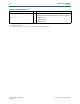
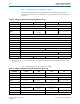
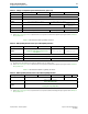
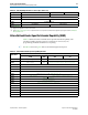
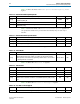
Table Of Contents
- Cyclone V Hard IP for PCI Express User Guide
- Contents
- 1. Datasheet
- 2. Getting Started with the Cyclone V Hard IP for PCI Express
- 3. Getting Started with the Avalon-MM Cyclone Hard IP for PCI Express
- Running Qsys
- Customizing the Cyclone VHard IP for PCI Express IP Core
- Adding the Remaining Components to the Qsys System
- Completing the Connections in Qsys
- Specifying Clocks and Interrupts
- Specifying Exported Interfaces
- Specifying Address Assignments
- Simulating the Example Design
- Simulating the Single DWord Design
- Understanding Channel Placement Guidelines
- Adding Synopsis Design Constraints
- Creating a Quartus II Project
- Compiling the Design
- Programming a Device
- 4. Parameter Settings for the Cyclone V Hard IP for PCI Express
- 5. Parameter Settings for the Avalon-MM Cyclone V Hard IP for PCI Express
- 6. IP Core Architecture
- Key Interfaces
- Protocol Layers
- Multi-Function Support
- PCI Express Avalon-MM Bridge
- Avalon-MM Bridge TLPs
- Avalon-MM-to-PCI Express Write Requests
- Avalon-MM-to-PCI Express Upstream Read Requests
- PCI Express-to-Avalon-MM Read Completions
- PCI Express-to-Avalon-MM Downstream Write Requests
- PCI Express-to-Avalon-MM Downstream Read Requests
- Avalon-MM-to-PCI Express Read Completions
- PCI Express-to-Avalon-MM Address Translation for Endpoints
- Minimizing BAR Sizes and the PCIe Address Space
- Avalon-MM-to-PCI Express Address Translation Algorithm
- Single DWord Completer Endpoint
- 7. IP Core Interfaces
- Cyclone V Hard IP for PCI Express
- Avalon-MM Hard IP for PCI Express
- Physical Layer Interface Signals
- Test Signals
- 8. Register Descriptions
- Configuration Space Register Content
- Altera-Defined Vendor Specific Extended Capability (VSEC)
- PCI Express Avalon-MM Bridge Control Register Access Content
- Avalon-MM to PCI Express Interrupt Registers
- PCI Express Mailbox Registers
- Avalon-MM-to-PCI Express Address Translation Table
- Root Port TLP Data Registers
- Programming Model for Avalon-MM Root Port
- PCI Express to Avalon-MM Interrupt Status and Enable Registers for Root Ports
- PCI Express to Avalon-MM Interrupt Status and Enable Registers for Endpoints
- Avalon-MM Mailbox Registers
- Correspondence between Configuration Space Registers and the PCIe Spec 2.1
- 9. Reset and Clocks
- 10. Transaction Layer Protocol (TLP) Details
- 11. Interrupts
- Interrupts for Endpoints Using the Avalon-ST Application Interface
- Interrupts for Root Ports Using the Avalon-ST Interface to the Application Layer
- Interrupts for Endpoints Using the Avalon-MM Interface to the Application Layer
- Interrupts for End Points Using the Avalon-MM Interface with Multiple MSI/MSI-X Support
- 12. Optional Features
- 13. Flow Control
- 14. Error Handling
- 15. Transceiver PHY IP Reconfiguration
- 16. SDC Timing Constraints
- 17. Testbench and Design Example
- Endpoint Testbench
- Root Port Testbench
- Chaining DMA Design Examples
- Test Driver Module
- Root Port Design Example
- Root Port BFM
- BFM Procedures and Functions
- 18. Debugging
- A. Transaction Layer Packet (TLP) Header Formats
- Additional Information

8–2 Chapter 8: Register Descriptions
Configuration Space Register Content
Cyclone V Hard IP for PCI Express December 2013 Altera Corporation
User Guide
Table 8–2 describes the Type 0 Configuration settings.
1 In the following tables, the names of fields that are defined by parameters in the
parameter editor are links to the description of that parameter. These links appear as
green text.
Table 8–3 describes the Type 1 Configuration settings.
Table 8–2. PCI Type 0 Configuration Space Header (Endpoints), Rev2.1
Byte Offset 31:24 23:16 15:8 7:0
0x000 Device ID Vendor ID
0x004
Status Command
0x008 Class code Revision ID
0x00C
0x00
Header Type
(
Port type
)
0x00 Cache Line Size
0x010 Func0–Func7 BARs and Expansion ROM
0x014 Func0–Func7 BARs and Expansion ROM
0x018 Func0–Func7 BARs and Expansion ROM
0x01C Func0–Func7 BARs and Expansion ROM
0x020 Func0–Func7 BARs and Expansion ROM
0x024 Func0–Func7 BARs and Expansion ROM
0x028 Reserved
0x02C Subsystem Device ID Subsystem Vendor ID
0x030 Expansion ROM base address
0x034 Reserved Capabilities Pointer
0x038 Reserved
0x03C 0x00 0x00 Interrupt Pin Interrupt Line
Note to Table 8–2:
(1) Refer to Table 8–39 on page 8–22 for a comprehensive list of correspondences between the Configuration Space registers and the PCI Express
Base Specification 2.1.
Table 8–3. PCI Type 1 Configuration Space Header (Root Ports) (Part 1 of 2)
Byte Offset 31:24 23:16 15:8 7:0
0x0000 Device ID Vendor ID
0x004
Status Command
0x008 Class code Revision ID
0x00C
BIST Header Type
Primary Latency
Timer
Cache Line Size
0x010 Reserved
0x014 Reserved
0x018
Secondary Latency
Timer
Subordinate Bus
Number
Secondary Bus
Number
Primary Bus Number
0x01C
Secondary Status I/O Limit I/O Base
0x020
Memory Limit Memory Base