
User guide

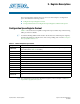
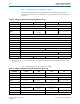
Table Of Contents
- Cyclone V Hard IP for PCI Express User Guide
- Contents
- 1. Datasheet
- 2. Getting Started with the Cyclone V Hard IP for PCI Express
- 3. Getting Started with the Avalon-MM Cyclone Hard IP for PCI Express
- Running Qsys
- Customizing the Cyclone VHard IP for PCI Express IP Core
- Adding the Remaining Components to the Qsys System
- Completing the Connections in Qsys
- Specifying Clocks and Interrupts
- Specifying Exported Interfaces
- Specifying Address Assignments
- Simulating the Example Design
- Simulating the Single DWord Design
- Understanding Channel Placement Guidelines
- Adding Synopsis Design Constraints
- Creating a Quartus II Project
- Compiling the Design
- Programming a Device
- 4. Parameter Settings for the Cyclone V Hard IP for PCI Express
- 5. Parameter Settings for the Avalon-MM Cyclone V Hard IP for PCI Express
- 6. IP Core Architecture
- Key Interfaces
- Protocol Layers
- Multi-Function Support
- PCI Express Avalon-MM Bridge
- Avalon-MM Bridge TLPs
- Avalon-MM-to-PCI Express Write Requests
- Avalon-MM-to-PCI Express Upstream Read Requests
- PCI Express-to-Avalon-MM Read Completions
- PCI Express-to-Avalon-MM Downstream Write Requests
- PCI Express-to-Avalon-MM Downstream Read Requests
- Avalon-MM-to-PCI Express Read Completions
- PCI Express-to-Avalon-MM Address Translation for Endpoints
- Minimizing BAR Sizes and the PCIe Address Space
- Avalon-MM-to-PCI Express Address Translation Algorithm
- Single DWord Completer Endpoint
- 7. IP Core Interfaces
- Cyclone V Hard IP for PCI Express
- Avalon-MM Hard IP for PCI Express
- Physical Layer Interface Signals
- Test Signals
- 8. Register Descriptions
- Configuration Space Register Content
- Altera-Defined Vendor Specific Extended Capability (VSEC)
- PCI Express Avalon-MM Bridge Control Register Access Content
- Avalon-MM to PCI Express Interrupt Registers
- PCI Express Mailbox Registers
- Avalon-MM-to-PCI Express Address Translation Table
- Root Port TLP Data Registers
- Programming Model for Avalon-MM Root Port
- PCI Express to Avalon-MM Interrupt Status and Enable Registers for Root Ports
- PCI Express to Avalon-MM Interrupt Status and Enable Registers for Endpoints
- Avalon-MM Mailbox Registers
- Correspondence between Configuration Space Registers and the PCIe Spec 2.1
- 9. Reset and Clocks
- 10. Transaction Layer Protocol (TLP) Details
- 11. Interrupts
- Interrupts for Endpoints Using the Avalon-ST Application Interface
- Interrupts for Root Ports Using the Avalon-ST Interface to the Application Layer
- Interrupts for Endpoints Using the Avalon-MM Interface to the Application Layer
- Interrupts for End Points Using the Avalon-MM Interface with Multiple MSI/MSI-X Support
- 12. Optional Features
- 13. Flow Control
- 14. Error Handling
- 15. Transceiver PHY IP Reconfiguration
- 16. SDC Timing Constraints
- 17. Testbench and Design Example
- Endpoint Testbench
- Root Port Testbench
- Chaining DMA Design Examples
- Test Driver Module
- Root Port Design Example
- Root Port BFM
- BFM Procedures and Functions
- 18. Debugging
- A. Transaction Layer Packet (TLP) Header Formats
- Additional Information
December 2013 Altera Corporation Cyclone V Hard IP for PCI Express
User Guide
8. Register Descriptions
This section describes registers that you can access the PCI Express Configuration
Space. It includes the following sections:
■ Configuration Space Register Content
■ Correspondence between Configuration Space Registers and the PCIe Spec 2.1
Configuration Space Register Content
Table 8–1 shows the PCI Compatible Configuration Space address map. The following
tables provide more details.
1 To facilitate finding additional information about these PCI and PCI Express registers,
the following tables provide the name of the corresponding section in the PCI Express
Base Specification Revision 2.1.
f For comprehensive information about these registers, refer to Chapter 7 of the PCI
Express Base Specification Revision 2.1.
Table 8–1. Common Configuration Space Header
Byte Offset Register Set
0x000:0x03C
PCI Type 0 Configuration Space Header (Refer to Table 8–2 for details) or PCI Type 1 Configuration
Space Header (Refer to Table 8–3 for details.)
0x040:0x04C Reserved.
0x050:0x05C MSI Capability Structure (Refer to Table 8–4 for details.)
0x060:0x064 Reserved
0x068:0x070 MSI-X Capability Structure (Refer to Table 8–5 for details.)
0x071:0x074 Reserved
0x078:0x07C Power Management Capability Structure (Refer to Table 8–6 for details.)
0x080:0x0BC PCI Express Capability Structure (Refer to Table 8–8 for details.)
0x0C0:0x0C4 Reserved
0x0C8-0x7FC Reserved
0x800:0x834 Advanced error reporting (AER) (optional)
0x838:0xFFF Reserved
0x100:0x16C
Virtual Channel Capability Structure for Function 0, Vendor Specific Extended Capability for Functions
1–7
December 2013
UG-01110-1.5