
User guide


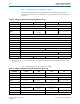
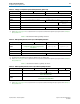

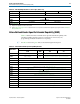
Table Of Contents
- Cyclone V Hard IP for PCI Express User Guide
- Contents
- 1. Datasheet
- 2. Getting Started with the Cyclone V Hard IP for PCI Express
- 3. Getting Started with the Avalon-MM Cyclone Hard IP for PCI Express
- Running Qsys
- Customizing the Cyclone VHard IP for PCI Express IP Core
- Adding the Remaining Components to the Qsys System
- Completing the Connections in Qsys
- Specifying Clocks and Interrupts
- Specifying Exported Interfaces
- Specifying Address Assignments
- Simulating the Example Design
- Simulating the Single DWord Design
- Understanding Channel Placement Guidelines
- Adding Synopsis Design Constraints
- Creating a Quartus II Project
- Compiling the Design
- Programming a Device
- 4. Parameter Settings for the Cyclone V Hard IP for PCI Express
- 5. Parameter Settings for the Avalon-MM Cyclone V Hard IP for PCI Express
- 6. IP Core Architecture
- Key Interfaces
- Protocol Layers
- Multi-Function Support
- PCI Express Avalon-MM Bridge
- Avalon-MM Bridge TLPs
- Avalon-MM-to-PCI Express Write Requests
- Avalon-MM-to-PCI Express Upstream Read Requests
- PCI Express-to-Avalon-MM Read Completions
- PCI Express-to-Avalon-MM Downstream Write Requests
- PCI Express-to-Avalon-MM Downstream Read Requests
- Avalon-MM-to-PCI Express Read Completions
- PCI Express-to-Avalon-MM Address Translation for Endpoints
- Minimizing BAR Sizes and the PCIe Address Space
- Avalon-MM-to-PCI Express Address Translation Algorithm
- Single DWord Completer Endpoint
- 7. IP Core Interfaces
- Cyclone V Hard IP for PCI Express
- Avalon-MM Hard IP for PCI Express
- Physical Layer Interface Signals
- Test Signals
- 8. Register Descriptions
- Configuration Space Register Content
- Altera-Defined Vendor Specific Extended Capability (VSEC)
- PCI Express Avalon-MM Bridge Control Register Access Content
- Avalon-MM to PCI Express Interrupt Registers
- PCI Express Mailbox Registers
- Avalon-MM-to-PCI Express Address Translation Table
- Root Port TLP Data Registers
- Programming Model for Avalon-MM Root Port
- PCI Express to Avalon-MM Interrupt Status and Enable Registers for Root Ports
- PCI Express to Avalon-MM Interrupt Status and Enable Registers for Endpoints
- Avalon-MM Mailbox Registers
- Correspondence between Configuration Space Registers and the PCIe Spec 2.1
- 9. Reset and Clocks
- 10. Transaction Layer Protocol (TLP) Details
- 11. Interrupts
- Interrupts for Endpoints Using the Avalon-ST Application Interface
- Interrupts for Root Ports Using the Avalon-ST Interface to the Application Layer
- Interrupts for Endpoints Using the Avalon-MM Interface to the Application Layer
- Interrupts for End Points Using the Avalon-MM Interface with Multiple MSI/MSI-X Support
- 12. Optional Features
- 13. Flow Control
- 14. Error Handling
- 15. Transceiver PHY IP Reconfiguration
- 16. SDC Timing Constraints
- 17. Testbench and Design Example
- Endpoint Testbench
- Root Port Testbench
- Chaining DMA Design Examples
- Test Driver Module
- Root Port Design Example
- Root Port BFM
- BFM Procedures and Functions
- 18. Debugging
- A. Transaction Layer Packet (TLP) Header Formats
- Additional Information

Chapter 7: IP Core Interfaces 7–55
Test Signals
December 2013 Altera Corporation Cyclone V Hard IP for PCI Express
User Guide
Test Signals
The
test_in
bus provides run-time control and monitoring of the internal state of the
Cyclone V Hard IP for PCI Express. Table 7–26 describes the test signals.
c Altera recommends that you use the
test_in
signals for debug or non-critical status
monitoring purposes such as LED displays of PCIe link status. They should not be
used for design function purposes. Use of these signals will make it more difficult to
close timing on the design. The test signals have not been rigorously verified and will
not function as documented in some corner cases.
Table 7–26 describes the
test_in
bus signals. In Qsys these signals have the prefix,
hip_ctrl_.
txmargin0[2:0]
O
Selects the TX V
OD
settings. The following settings are defined:
■ 3'b000: Normal operating range
■ 3'b001: Full swing: 800 - 1200 mV, Half swing: 400 - 700 mV
■ 3'b010: Reserved
■ 3'b011: Reserved
■ 3'b100: Full swing: 200 - 400 mV Half swing: 100 - 200 mV if the last
value or vendor defined
■ 3'b101: Full swing: 200 - 400 mV Half swing: 100 - 200 mV
■ 3'b110: Full swing: 200 - 400 mV Half swing: 100 - 200 mV
■ 3'b111: Full swing: 200 - 400 mV, Half swing: 100 - 200 mV
Notes to Table 7–25:
(1) Signals that include lane number 0 also exist for lanes 1-7.
(2) These signals are for simulation only. For Quartus II software compilation, these pipe signals can be left floating.
Table 7–25. PIPE Interface Signals (Part 4 of 4)
Signal I/O Description
Table 7–26. Test Interface Signals
(1)
,
(2)
Signal I/O Description
test_in[31:0]
I
[0]–Simulation mode. This signal can be set to 1 to accelerate
initialization by reducing the value of many initialization counters.
[4:1] Reserved. Must be set to 4’b0100.
[6:5] Compliance test mode. Disable/force compliance mode:
■ bit 0–When set, prevents the LTSSM from entering compliance
mode. Toggling this bit controls the entry and exit from the
compliance state, enabling the transmission of Gen1 and Gen2
compliance patterns.
■ bit 1–Forces compliance mode. Forces entry to compliance mode
when timeout is reached in polling.active state (and not all lanes
have detected their exit condition).
■ [31:7] Reserved.
simu_mode_pipe
O When set to 1, the PIPE interface is in simulation mode.