
User guide

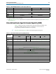
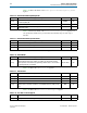
Table Of Contents
- Cyclone V Hard IP for PCI Express User Guide
- Contents
- 1. Datasheet
- 2. Getting Started with the Cyclone V Hard IP for PCI Express
- 3. Getting Started with the Avalon-MM Cyclone Hard IP for PCI Express
- Running Qsys
- Customizing the Cyclone VHard IP for PCI Express IP Core
- Adding the Remaining Components to the Qsys System
- Completing the Connections in Qsys
- Specifying Clocks and Interrupts
- Specifying Exported Interfaces
- Specifying Address Assignments
- Simulating the Example Design
- Simulating the Single DWord Design
- Understanding Channel Placement Guidelines
- Adding Synopsis Design Constraints
- Creating a Quartus II Project
- Compiling the Design
- Programming a Device
- 4. Parameter Settings for the Cyclone V Hard IP for PCI Express
- 5. Parameter Settings for the Avalon-MM Cyclone V Hard IP for PCI Express
- 6. IP Core Architecture
- Key Interfaces
- Protocol Layers
- Multi-Function Support
- PCI Express Avalon-MM Bridge
- Avalon-MM Bridge TLPs
- Avalon-MM-to-PCI Express Write Requests
- Avalon-MM-to-PCI Express Upstream Read Requests
- PCI Express-to-Avalon-MM Read Completions
- PCI Express-to-Avalon-MM Downstream Write Requests
- PCI Express-to-Avalon-MM Downstream Read Requests
- Avalon-MM-to-PCI Express Read Completions
- PCI Express-to-Avalon-MM Address Translation for Endpoints
- Minimizing BAR Sizes and the PCIe Address Space
- Avalon-MM-to-PCI Express Address Translation Algorithm
- Single DWord Completer Endpoint
- 7. IP Core Interfaces
- Cyclone V Hard IP for PCI Express
- Avalon-MM Hard IP for PCI Express
- Physical Layer Interface Signals
- Test Signals
- 8. Register Descriptions
- Configuration Space Register Content
- Altera-Defined Vendor Specific Extended Capability (VSEC)
- PCI Express Avalon-MM Bridge Control Register Access Content
- Avalon-MM to PCI Express Interrupt Registers
- PCI Express Mailbox Registers
- Avalon-MM-to-PCI Express Address Translation Table
- Root Port TLP Data Registers
- Programming Model for Avalon-MM Root Port
- PCI Express to Avalon-MM Interrupt Status and Enable Registers for Root Ports
- PCI Express to Avalon-MM Interrupt Status and Enable Registers for Endpoints
- Avalon-MM Mailbox Registers
- Correspondence between Configuration Space Registers and the PCIe Spec 2.1
- 9. Reset and Clocks
- 10. Transaction Layer Protocol (TLP) Details
- 11. Interrupts
- Interrupts for Endpoints Using the Avalon-ST Application Interface
- Interrupts for Root Ports Using the Avalon-ST Interface to the Application Layer
- Interrupts for Endpoints Using the Avalon-MM Interface to the Application Layer
- Interrupts for End Points Using the Avalon-MM Interface with Multiple MSI/MSI-X Support
- 12. Optional Features
- 13. Flow Control
- 14. Error Handling
- 15. Transceiver PHY IP Reconfiguration
- 16. SDC Timing Constraints
- 17. Testbench and Design Example
- Endpoint Testbench
- Root Port Testbench
- Chaining DMA Design Examples
- Test Driver Module
- Root Port Design Example
- Root Port BFM
- BFM Procedures and Functions
- 18. Debugging
- A. Transaction Layer Packet (TLP) Header Formats
- Additional Information

Chapter 7: IP Core Interfaces 7–53
Physical Layer Interface Signals
December 2013 Altera Corporation Cyclone V Hard IP for PCI Express
User Guide
txcompl0
(1)
O
Transmit compliance
<
n>. This signal forces the running disparity to
negative in compliance mode (negative COM character).
rxpolarity0
(1)
O
Receive polarity
<
n>. This signal instructs the PHY layer to invert the
polarity of the 8B/10B receiver decoding block.
powerdown0[1:0]
(1)
O
Power down
<
n>. This signal requests the PHY to change its power state
to the specified state (P0, P0s, P1, or P2).
tx_deemph0
O
Transmit de-emphasis selection. The Cyclone V Hard IP for PCI Express
sets the value for this signal based on the indication received from the
other end of the link during the Training Sequences (TS). You do not
need to change this value.
rxdata0[7:0]
(1) (2)
I Receive data
<
n>. This bus receives data on lane
<
n>.
rxdatak0[1:0]
(1) (2)
I
Receive data control
<
n>. This signal separates control and data
symbols.
rxvalid0
(1) (2)
I
Receive valid
<
n>. This symbol indicates symbol lock and valid data on
rxdata<
n> and
rxdatak<
n>.
phystatus0
(1) (2)
I
PHY status
<
n>. This signal communicates completion of several PHY
requests.
eidleinfersel0[2:0]
O
Electrical idle entry inference mechanism selection. The following
encodings are defined:
■ 3'b0xx: Electrical Idle Inference not required in current LTSSM state
■ 3'b100: Absence of COM/SKP Ordered Set the in 128 us window for
Gen1 or Gen2
■ 3'b101: Absence of TS1/TS2 Ordered Set in a 1280 UI interval for
Gen1 or Gen2
■ 3'b110: Absence of Electrical Idle Exit in 2000 UI interval for Gen1 and
16000 UI interval for Gen2
■ 3'b111: Absence of Electrical idle exit in 128 us window for Gen1
rxelecidle0
(1) (2)
I
Receive electrical idle
<
n>. This signal forces the receive output to
electrical idle.
rxstatus0[2:0]
(1) (2)
I
Receive status
<
n>. This signal encodes receive status and error codes
for the receive data stream and receiver detection.
Table 7–25. PIPE Interface Signals (Part 2 of 4)
Signal I/O Description