
User guide
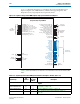
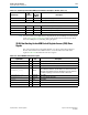
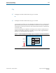

Table Of Contents
- Cyclone V Hard IP for PCI Express User Guide
- Contents
- 1. Datasheet
- 2. Getting Started with the Cyclone V Hard IP for PCI Express
- 3. Getting Started with the Avalon-MM Cyclone Hard IP for PCI Express
- Running Qsys
- Customizing the Cyclone VHard IP for PCI Express IP Core
- Adding the Remaining Components to the Qsys System
- Completing the Connections in Qsys
- Specifying Clocks and Interrupts
- Specifying Exported Interfaces
- Specifying Address Assignments
- Simulating the Example Design
- Simulating the Single DWord Design
- Understanding Channel Placement Guidelines
- Adding Synopsis Design Constraints
- Creating a Quartus II Project
- Compiling the Design
- Programming a Device
- 4. Parameter Settings for the Cyclone V Hard IP for PCI Express
- 5. Parameter Settings for the Avalon-MM Cyclone V Hard IP for PCI Express
- 6. IP Core Architecture
- Key Interfaces
- Protocol Layers
- Multi-Function Support
- PCI Express Avalon-MM Bridge
- Avalon-MM Bridge TLPs
- Avalon-MM-to-PCI Express Write Requests
- Avalon-MM-to-PCI Express Upstream Read Requests
- PCI Express-to-Avalon-MM Read Completions
- PCI Express-to-Avalon-MM Downstream Write Requests
- PCI Express-to-Avalon-MM Downstream Read Requests
- Avalon-MM-to-PCI Express Read Completions
- PCI Express-to-Avalon-MM Address Translation for Endpoints
- Minimizing BAR Sizes and the PCIe Address Space
- Avalon-MM-to-PCI Express Address Translation Algorithm
- Single DWord Completer Endpoint
- 7. IP Core Interfaces
- Cyclone V Hard IP for PCI Express
- Avalon-MM Hard IP for PCI Express
- Physical Layer Interface Signals
- Test Signals
- 8. Register Descriptions
- Configuration Space Register Content
- Altera-Defined Vendor Specific Extended Capability (VSEC)
- PCI Express Avalon-MM Bridge Control Register Access Content
- Avalon-MM to PCI Express Interrupt Registers
- PCI Express Mailbox Registers
- Avalon-MM-to-PCI Express Address Translation Table
- Root Port TLP Data Registers
- Programming Model for Avalon-MM Root Port
- PCI Express to Avalon-MM Interrupt Status and Enable Registers for Root Ports
- PCI Express to Avalon-MM Interrupt Status and Enable Registers for Endpoints
- Avalon-MM Mailbox Registers
- Correspondence between Configuration Space Registers and the PCIe Spec 2.1
- 9. Reset and Clocks
- 10. Transaction Layer Protocol (TLP) Details
- 11. Interrupts
- Interrupts for Endpoints Using the Avalon-ST Application Interface
- Interrupts for Root Ports Using the Avalon-ST Interface to the Application Layer
- Interrupts for Endpoints Using the Avalon-MM Interface to the Application Layer
- Interrupts for End Points Using the Avalon-MM Interface with Multiple MSI/MSI-X Support
- 12. Optional Features
- 13. Flow Control
- 14. Error Handling
- 15. Transceiver PHY IP Reconfiguration
- 16. SDC Timing Constraints
- 17. Testbench and Design Example
- Endpoint Testbench
- Root Port Testbench
- Chaining DMA Design Examples
- Test Driver Module
- Root Port Design Example
- Root Port BFM
- BFM Procedures and Functions
- 18. Debugging
- A. Transaction Layer Packet (TLP) Header Formats
- Additional Information
7–52 Chapter 7: IP Core Interfaces
Physical Layer Interface Signals
Cyclone V Hard IP for PCI Express December 2013 Altera Corporation
User Guide
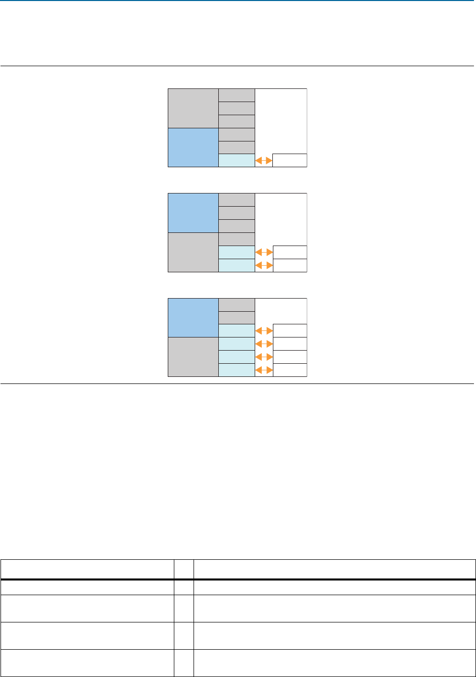
1 In all figures channels and PLLs that are gray are unused.
PIPE Interface Signals
The PIPE signals are available so that you can simulate using either the one-bit or the
PIPE interface. Simulation is much faster using the PIPE interface. You can use the 8-
bit PIPE interface for simulation even though your actual design includes the serial
interface to the internal transceivers. However, it is not possible to use the Hard IP
PIPE interface in an actual device. Table 7–25 describes the PIPE interface signals used
for a standard 16-bit SDR or 8-bit SDR interface. In Table 7–25, signals that include
lane number 0 also exist for lanes 1-7. In Qsys, the signals that are part of the PIPE
interface have the prefix, hip_pipe. The signals which are included to simulate the PIPE
interface have the prefix, hip_pipe_sim_pipe.
Figure 7–38. Channel Placement Using ATX PLL
&K
&K
&K
&K
&K
$7;3//
&K
3&,H+DUG,3
$7;3//
&K
&K
&K
&K
&K
&K
$7;3//
&K$7;3//
3&,H+DUG,3
&K
&K
&K
&K
&K
&K
&K
$7;3//
&K
3&,H+DUG,3
$7;3//
&K
&K
&K
&K
[
[
[
Table 7–25. PIPE Interface Signals (Part 1 of 4)
Signal I/O Description
txdata0[7:0]
O Transmit data
<
n>. This bus transmits data on lane
<
n>.
txdatak0
(1)
O
Transmit data control
<
n>. This signal serves as the control bit for
txdata<
n>.
txdetectrx0
(1)
O
Transmit detect receive
<
n>. This signal tells the PHY layer to start a
receive detection operation or to begin loopback.
txelecidle
(1)
O
Transmit electrical idle
<
n>. This signal forces the TX output to electrical
idle.