
User guide
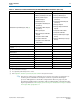

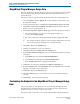
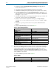
Table Of Contents
- Cyclone V Hard IP for PCI Express User Guide
- Contents
- 1. Datasheet
- 2. Getting Started with the Cyclone V Hard IP for PCI Express
- 3. Getting Started with the Avalon-MM Cyclone Hard IP for PCI Express
- Running Qsys
- Customizing the Cyclone VHard IP for PCI Express IP Core
- Adding the Remaining Components to the Qsys System
- Completing the Connections in Qsys
- Specifying Clocks and Interrupts
- Specifying Exported Interfaces
- Specifying Address Assignments
- Simulating the Example Design
- Simulating the Single DWord Design
- Understanding Channel Placement Guidelines
- Adding Synopsis Design Constraints
- Creating a Quartus II Project
- Compiling the Design
- Programming a Device
- 4. Parameter Settings for the Cyclone V Hard IP for PCI Express
- 5. Parameter Settings for the Avalon-MM Cyclone V Hard IP for PCI Express
- 6. IP Core Architecture
- Key Interfaces
- Protocol Layers
- Multi-Function Support
- PCI Express Avalon-MM Bridge
- Avalon-MM Bridge TLPs
- Avalon-MM-to-PCI Express Write Requests
- Avalon-MM-to-PCI Express Upstream Read Requests
- PCI Express-to-Avalon-MM Read Completions
- PCI Express-to-Avalon-MM Downstream Write Requests
- PCI Express-to-Avalon-MM Downstream Read Requests
- Avalon-MM-to-PCI Express Read Completions
- PCI Express-to-Avalon-MM Address Translation for Endpoints
- Minimizing BAR Sizes and the PCIe Address Space
- Avalon-MM-to-PCI Express Address Translation Algorithm
- Single DWord Completer Endpoint
- 7. IP Core Interfaces
- Cyclone V Hard IP for PCI Express
- Avalon-MM Hard IP for PCI Express
- Physical Layer Interface Signals
- Test Signals
- 8. Register Descriptions
- Configuration Space Register Content
- Altera-Defined Vendor Specific Extended Capability (VSEC)
- PCI Express Avalon-MM Bridge Control Register Access Content
- Avalon-MM to PCI Express Interrupt Registers
- PCI Express Mailbox Registers
- Avalon-MM-to-PCI Express Address Translation Table
- Root Port TLP Data Registers
- Programming Model for Avalon-MM Root Port
- PCI Express to Avalon-MM Interrupt Status and Enable Registers for Root Ports
- PCI Express to Avalon-MM Interrupt Status and Enable Registers for Endpoints
- Avalon-MM Mailbox Registers
- Correspondence between Configuration Space Registers and the PCIe Spec 2.1
- 9. Reset and Clocks
- 10. Transaction Layer Protocol (TLP) Details
- 11. Interrupts
- Interrupts for Endpoints Using the Avalon-ST Application Interface
- Interrupts for Root Ports Using the Avalon-ST Interface to the Application Layer
- Interrupts for Endpoints Using the Avalon-MM Interface to the Application Layer
- Interrupts for End Points Using the Avalon-MM Interface with Multiple MSI/MSI-X Support
- 12. Optional Features
- 13. Flow Control
- 14. Error Handling
- 15. Transceiver PHY IP Reconfiguration
- 16. SDC Timing Constraints
- 17. Testbench and Design Example
- Endpoint Testbench
- Root Port Testbench
- Chaining DMA Design Examples
- Test Driver Module
- Root Port Design Example
- Root Port BFM
- BFM Procedures and Functions
- 18. Debugging
- A. Transaction Layer Packet (TLP) Header Formats
- Additional Information

Chapter 1: Datasheet 1–7
Recommended Speed Grades
December 2013 Altera Corporation Cyclone V Hard IP for PCI Express
User Guide
Soft calibration of the transceiver module requires additional logic. The amount of
logic required depends upon the configuration.
Recommended Speed Grades
Table 1–6 lists the recommended speed grades for the supported link widths and
Application Layer clock frequencies. The speed grades listed are the only speed
grades that close timing. Altera recommends setting the Quartus II Analysis &
Synthesis Settings Optimization Technique to Speed.
h For information about optimizing synthesis, refer to “Setting Up and Running Analysis
and Synthesis in Quartus II Help.
For more information about how to effect the Optimization Technique settings, refer
to Area and Timing Optimization in volume 2 of the Quartus II Handbook.
f For details on installation, refer to the Altera Software Installation and Licensing Manual.
Table 1–5. Device Family Link Width Application Frequency Recommended Speed Grades
Link Speed Link Width
Application
Clock
Frequency (MHz)
Recommended
Speed Grades
Gen1–2.5 Gbps
×1 62.5
(1)
–6, -7, -8
(2)
×1 125 –6, -7, -8
×2 125 –6
×4 125 –6, -7, -8
Gen2–5.0 Gbps
×1 62.5
(1)
,–6, -7
(2)
×1 125 –6, -7,
(2)
×2 125 ,–6, -7
(2)
×4 125 –6, -7,
(2)
Notes to Table 1–6:
(1) This is a power-saving mode of operation.
(2) Final results pending characterization by Altera. Refer to the fit.rpt file generated by the Quartus II software.