
User guide
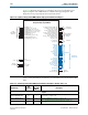
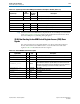
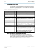
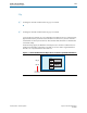
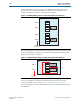
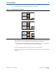
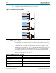
Table Of Contents
- Cyclone V Hard IP for PCI Express User Guide
- Contents
- 1. Datasheet
- 2. Getting Started with the Cyclone V Hard IP for PCI Express
- 3. Getting Started with the Avalon-MM Cyclone Hard IP for PCI Express
- Running Qsys
- Customizing the Cyclone VHard IP for PCI Express IP Core
- Adding the Remaining Components to the Qsys System
- Completing the Connections in Qsys
- Specifying Clocks and Interrupts
- Specifying Exported Interfaces
- Specifying Address Assignments
- Simulating the Example Design
- Simulating the Single DWord Design
- Understanding Channel Placement Guidelines
- Adding Synopsis Design Constraints
- Creating a Quartus II Project
- Compiling the Design
- Programming a Device
- 4. Parameter Settings for the Cyclone V Hard IP for PCI Express
- 5. Parameter Settings for the Avalon-MM Cyclone V Hard IP for PCI Express
- 6. IP Core Architecture
- Key Interfaces
- Protocol Layers
- Multi-Function Support
- PCI Express Avalon-MM Bridge
- Avalon-MM Bridge TLPs
- Avalon-MM-to-PCI Express Write Requests
- Avalon-MM-to-PCI Express Upstream Read Requests
- PCI Express-to-Avalon-MM Read Completions
- PCI Express-to-Avalon-MM Downstream Write Requests
- PCI Express-to-Avalon-MM Downstream Read Requests
- Avalon-MM-to-PCI Express Read Completions
- PCI Express-to-Avalon-MM Address Translation for Endpoints
- Minimizing BAR Sizes and the PCIe Address Space
- Avalon-MM-to-PCI Express Address Translation Algorithm
- Single DWord Completer Endpoint
- 7. IP Core Interfaces
- Cyclone V Hard IP for PCI Express
- Avalon-MM Hard IP for PCI Express
- Physical Layer Interface Signals
- Test Signals
- 8. Register Descriptions
- Configuration Space Register Content
- Altera-Defined Vendor Specific Extended Capability (VSEC)
- PCI Express Avalon-MM Bridge Control Register Access Content
- Avalon-MM to PCI Express Interrupt Registers
- PCI Express Mailbox Registers
- Avalon-MM-to-PCI Express Address Translation Table
- Root Port TLP Data Registers
- Programming Model for Avalon-MM Root Port
- PCI Express to Avalon-MM Interrupt Status and Enable Registers for Root Ports
- PCI Express to Avalon-MM Interrupt Status and Enable Registers for Endpoints
- Avalon-MM Mailbox Registers
- Correspondence between Configuration Space Registers and the PCIe Spec 2.1
- 9. Reset and Clocks
- 10. Transaction Layer Protocol (TLP) Details
- 11. Interrupts
- Interrupts for Endpoints Using the Avalon-ST Application Interface
- Interrupts for Root Ports Using the Avalon-ST Interface to the Application Layer
- Interrupts for Endpoints Using the Avalon-MM Interface to the Application Layer
- Interrupts for End Points Using the Avalon-MM Interface with Multiple MSI/MSI-X Support
- 12. Optional Features
- 13. Flow Control
- 14. Error Handling
- 15. Transceiver PHY IP Reconfiguration
- 16. SDC Timing Constraints
- 17. Testbench and Design Example
- Endpoint Testbench
- Root Port Testbench
- Chaining DMA Design Examples
- Test Driver Module
- Root Port Design Example
- Root Port BFM
- BFM Procedures and Functions
- 18. Debugging
- A. Transaction Layer Packet (TLP) Header Formats
- Additional Information
7–50 Chapter 7: IP Core Interfaces
Physical Layer Interface Signals
Cyclone V Hard IP for PCI Express December 2013 Altera Corporation
User Guide
The following figure shows the location of the Hard IP for PCI Express IP Cores in
devices with 9 or 12 channels. The Hard IP for PCI Express uses channel 1 and
channel 2 of GXB_L0 and channel 1 and channel 1of GXB_L2.
The following figure shows the location of the Hard IP for PCI Express IP Cores for ×4
variants. The Hard IP for PCI Express uses channel 1 and channel 2 of GXB_L0 and
channel 4 and channel 5 of GXB_L1.
For more comprehensive information about CycloneV transceivers refer to the
“Transceiver Banks” section in the Transceiver Architecture in Cyclone V Devices.
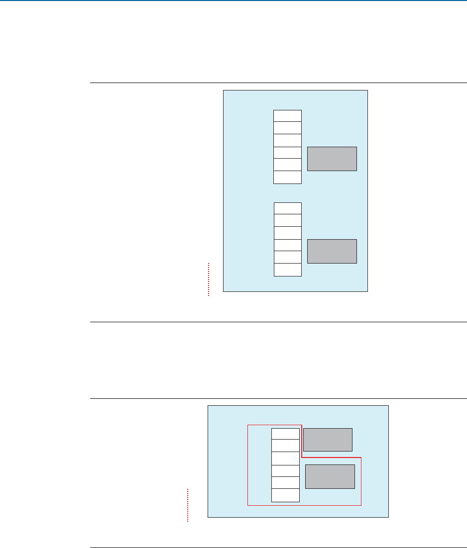
The following figures show the channel utilization for Gen1 and Gen2 variants using
the CMU PLL.
Figure 7–2. GX/GT/ST/ST Devices with 9 or 12 Transceiver Channels and 2 PCIe Cores
Figure 7–3. GX/GT/ST/ST Devices with 9 or 12 Transceiver Channels and 2 PCIe Cores
GXB_L1
GXB_L0
Transceiver
Bank Names
PCIe Hard IP
with CvP
Ch 2
Ch 1
Ch 0
Ch 5
Ch 4
Ch 3
PCIe Hard IP
GXB_L2
Ch 2
Ch 1
Ch 0
Ch 5
Ch 4
Ch 3
GXB_L3
GXB_L1
GXB_L0
Transceiver
Bank Names
PCIe Hard IP
Ch 2
Ch 1
Ch 0
Ch 5
Ch 4
Ch 3
6 Ch
6 Ch
PCIe Hard IP