
User guide
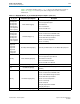
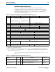
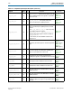


Table Of Contents
- Cyclone V Hard IP for PCI Express User Guide
- Contents
- 1. Datasheet
- 2. Getting Started with the Cyclone V Hard IP for PCI Express
- 3. Getting Started with the Avalon-MM Cyclone Hard IP for PCI Express
- Running Qsys
- Customizing the Cyclone VHard IP for PCI Express IP Core
- Adding the Remaining Components to the Qsys System
- Completing the Connections in Qsys
- Specifying Clocks and Interrupts
- Specifying Exported Interfaces
- Specifying Address Assignments
- Simulating the Example Design
- Simulating the Single DWord Design
- Understanding Channel Placement Guidelines
- Adding Synopsis Design Constraints
- Creating a Quartus II Project
- Compiling the Design
- Programming a Device
- 4. Parameter Settings for the Cyclone V Hard IP for PCI Express
- 5. Parameter Settings for the Avalon-MM Cyclone V Hard IP for PCI Express
- 6. IP Core Architecture
- Key Interfaces
- Protocol Layers
- Multi-Function Support
- PCI Express Avalon-MM Bridge
- Avalon-MM Bridge TLPs
- Avalon-MM-to-PCI Express Write Requests
- Avalon-MM-to-PCI Express Upstream Read Requests
- PCI Express-to-Avalon-MM Read Completions
- PCI Express-to-Avalon-MM Downstream Write Requests
- PCI Express-to-Avalon-MM Downstream Read Requests
- Avalon-MM-to-PCI Express Read Completions
- PCI Express-to-Avalon-MM Address Translation for Endpoints
- Minimizing BAR Sizes and the PCIe Address Space
- Avalon-MM-to-PCI Express Address Translation Algorithm
- Single DWord Completer Endpoint
- 7. IP Core Interfaces
- Cyclone V Hard IP for PCI Express
- Avalon-MM Hard IP for PCI Express
- Physical Layer Interface Signals
- Test Signals
- 8. Register Descriptions
- Configuration Space Register Content
- Altera-Defined Vendor Specific Extended Capability (VSEC)
- PCI Express Avalon-MM Bridge Control Register Access Content
- Avalon-MM to PCI Express Interrupt Registers
- PCI Express Mailbox Registers
- Avalon-MM-to-PCI Express Address Translation Table
- Root Port TLP Data Registers
- Programming Model for Avalon-MM Root Port
- PCI Express to Avalon-MM Interrupt Status and Enable Registers for Root Ports
- PCI Express to Avalon-MM Interrupt Status and Enable Registers for Endpoints
- Avalon-MM Mailbox Registers
- Correspondence between Configuration Space Registers and the PCIe Spec 2.1
- 9. Reset and Clocks
- 10. Transaction Layer Protocol (TLP) Details
- 11. Interrupts
- Interrupts for Endpoints Using the Avalon-ST Application Interface
- Interrupts for Root Ports Using the Avalon-ST Interface to the Application Layer
- Interrupts for Endpoints Using the Avalon-MM Interface to the Application Layer
- Interrupts for End Points Using the Avalon-MM Interface with Multiple MSI/MSI-X Support
- 12. Optional Features
- 13. Flow Control
- 14. Error Handling
- 15. Transceiver PHY IP Reconfiguration
- 16. SDC Timing Constraints
- 17. Testbench and Design Example
- Endpoint Testbench
- Root Port Testbench
- Chaining DMA Design Examples
- Test Driver Module
- Root Port Design Example
- Root Port BFM
- BFM Procedures and Functions
- 18. Debugging
- A. Transaction Layer Packet (TLP) Header Formats
- Additional Information

7–38 Chapter 7: IP Core Interfaces
Cyclone V Hard IP for PCI Express
Cyclone V Hard IP for PCI Express December 2013 Altera Corporation
User Guide
f Refer to the PCI Local Bus Specification for descriptions of the Control registers.
Table 7–14 describes the use of the various fields of the Configuration MSI Control
and Status Register.
cfg_msi_data
16 O
cfg_msi_data[15:0]
is message data for MSI.
Table 9–4 on
page 9–3
0x050
cfg_busdev
13 O
Bus/Device Number captured by or programmed in the
Hard IP.
Table A–5 on
page A–2
0x08
Table 7–13. Configuration Space Register Descriptions (Part 4 of 4)
Register
Width Dir Description
Register
Reference
Table 7–14. Configuration MSI Control Register Field Descriptions
Bit(s) Field Description
[15:9]
reserved
—
[8]
mask
capability
Per vector masking capable. This bit is hardwired to 0 because the functions do not
support the optional MSI per vector masking using the
Mask_Bits
and
Pending_Bits
registers defined in the PCI Local Bus Specification, Rev. 3.0. Per
vector masking can be implemented using Application Layer registers.
[7]
64-bit
address
capability
64-bit address capable
■ 1: function capable of sending a 64-bit message address
■ 0: function not capable of sending a 64-bit message address
[6:4]
multiples
message
enable
Multiple message enable: This field indicates permitted values for MSI signals. For
example, if “100” is written to this field 16 MSI signals are allocated
■ 000: 1 MSI allocated
■ 001: 2 MSI allocated
■ 010: 4 MSI allocated
■ 011: 8 MSI allocated
■ 100: 16 MSI allocated
■ 101: 32 MSI allocated
■ 110: Reserved
■ 111: Reserved
[3:1]
multiple
message
capable
Multiple message capable: This field is read by system software to determine the
number of requested MSI messages.
■ 000: 1 MSI requested
■ 001: 2 MSI requested
■ 010: 4 MSI requested
■ 011: 8 MSI requested
■ 100: 16 MSI requested
■ 101: 32 MSI requested
■ 110: Reserved
[0]
MSI Enable
If set to 0, this component is not permitted to use MSI.