
User guide
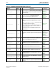
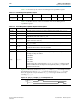
Table Of Contents
- Cyclone V Hard IP for PCI Express User Guide
- Contents
- 1. Datasheet
- 2. Getting Started with the Cyclone V Hard IP for PCI Express
- 3. Getting Started with the Avalon-MM Cyclone Hard IP for PCI Express
- Running Qsys
- Customizing the Cyclone VHard IP for PCI Express IP Core
- Adding the Remaining Components to the Qsys System
- Completing the Connections in Qsys
- Specifying Clocks and Interrupts
- Specifying Exported Interfaces
- Specifying Address Assignments
- Simulating the Example Design
- Simulating the Single DWord Design
- Understanding Channel Placement Guidelines
- Adding Synopsis Design Constraints
- Creating a Quartus II Project
- Compiling the Design
- Programming a Device
- 4. Parameter Settings for the Cyclone V Hard IP for PCI Express
- 5. Parameter Settings for the Avalon-MM Cyclone V Hard IP for PCI Express
- 6. IP Core Architecture
- Key Interfaces
- Protocol Layers
- Multi-Function Support
- PCI Express Avalon-MM Bridge
- Avalon-MM Bridge TLPs
- Avalon-MM-to-PCI Express Write Requests
- Avalon-MM-to-PCI Express Upstream Read Requests
- PCI Express-to-Avalon-MM Read Completions
- PCI Express-to-Avalon-MM Downstream Write Requests
- PCI Express-to-Avalon-MM Downstream Read Requests
- Avalon-MM-to-PCI Express Read Completions
- PCI Express-to-Avalon-MM Address Translation for Endpoints
- Minimizing BAR Sizes and the PCIe Address Space
- Avalon-MM-to-PCI Express Address Translation Algorithm
- Single DWord Completer Endpoint
- 7. IP Core Interfaces
- Cyclone V Hard IP for PCI Express
- Avalon-MM Hard IP for PCI Express
- Physical Layer Interface Signals
- Test Signals
- 8. Register Descriptions
- Configuration Space Register Content
- Altera-Defined Vendor Specific Extended Capability (VSEC)
- PCI Express Avalon-MM Bridge Control Register Access Content
- Avalon-MM to PCI Express Interrupt Registers
- PCI Express Mailbox Registers
- Avalon-MM-to-PCI Express Address Translation Table
- Root Port TLP Data Registers
- Programming Model for Avalon-MM Root Port
- PCI Express to Avalon-MM Interrupt Status and Enable Registers for Root Ports
- PCI Express to Avalon-MM Interrupt Status and Enable Registers for Endpoints
- Avalon-MM Mailbox Registers
- Correspondence between Configuration Space Registers and the PCIe Spec 2.1
- 9. Reset and Clocks
- 10. Transaction Layer Protocol (TLP) Details
- 11. Interrupts
- Interrupts for Endpoints Using the Avalon-ST Application Interface
- Interrupts for Root Ports Using the Avalon-ST Interface to the Application Layer
- Interrupts for Endpoints Using the Avalon-MM Interface to the Application Layer
- Interrupts for End Points Using the Avalon-MM Interface with Multiple MSI/MSI-X Support
- 12. Optional Features
- 13. Flow Control
- 14. Error Handling
- 15. Transceiver PHY IP Reconfiguration
- 16. SDC Timing Constraints
- 17. Testbench and Design Example
- Endpoint Testbench
- Root Port Testbench
- Chaining DMA Design Examples
- Test Driver Module
- Root Port Design Example
- Root Port BFM
- BFM Procedures and Functions
- 18. Debugging
- A. Transaction Layer Packet (TLP) Header Formats
- Additional Information

Chapter 7: IP Core Interfaces 7–37
Cyclone V Hard IP for PCI Express
December 2013 Altera Corporation Cyclone V Hard IP for PCI Express
User Guide
cfg_io_lim
20 O
The upper 20 bits of the IO limit registers of the Type1
Configuration Space. This register is only available in Root
Port mode.
Table 8–8 on
page 8–4
0x01C
cfg_np_bas
12 O
The upper 12 bits of the memory base register of the Type1
Configuration Space. This register is only available in Root
Port mode.
Table 4–7 on
page 4–8
EXP ROM
cfg_np_lim
12 O
The upper 12 bits of the memory limit register of the Type1
Configuration Space. This register is only available in Root
Port mode.
Table 4–7 on
page 4–8
EXP ROM
cfg_pr_bas
44 O
The upper 44 bits of the prefetchable base registers of the
Type1 Configuration Space. This register is only available in
Root Port mode.
Table 8–3 on
page 8–2
0x024 and
Table 4–7 on
page 4–8
Prefetchable
memory
cfg_pr_lim
44 O
The upper 44 bits of the prefetchable limit registers of the
Type1 Configuration Space. Available in Root Port mode.
Table 8–3 on
page 8–2
0x024 and
Table 4–7 on
page 4–8
Prefetchable
memory
cfg_pmcsr
32 O
cfg_pmcsr[31:16]
is Power Management Control and
cfg_pmcsr[15:0]
is the Power Management Status
register.
Table 8–6 on
page 8–4
0x07C
cfg_msix
16 O MSI-X message control.
Table 8–5 on
page 8–3
0x068
cfg_msi
16 O
MSI message control. Refer to Table 7–14 for the fields of
this register.
Table 8–4 on
page 8–3
0x050
cfg_tcvcmap
24 O
Configuration traffic class (TC)/virtual channel (VC)
mapping. The Application Layer uses this signal to generate
a TLP mapped to the appropriate channel based on the
traffic class of the packet.
cfg_tcvcmap[2:0]
: Mapping for TC0 (always 0).
cfg_tcvcmap[5:3]
: Mapping for TC1.
cfg_tcvcmap[8:6]
: Mapping for TC2.
cfg_tcvcmap[11:9]
: Mapping for TC3.
cfg_tcvcmap[14:12]
: Mapping for TC4.
cfg_tcvcmap[17:15]
: Mapping for TC5.
cfg_tcvcmap[20:18]
: Mapping for TC6.
cfg_tcvcmap[23:21]
: Mapping for TC7.
—
Table 7–13. Configuration Space Register Descriptions (Part 3 of 4)
Register
Width Dir Description
Register
Reference