
User guide
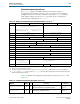
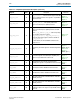
Table Of Contents
- Cyclone V Hard IP for PCI Express User Guide
- Contents
- 1. Datasheet
- 2. Getting Started with the Cyclone V Hard IP for PCI Express
- 3. Getting Started with the Avalon-MM Cyclone Hard IP for PCI Express
- Running Qsys
- Customizing the Cyclone VHard IP for PCI Express IP Core
- Adding the Remaining Components to the Qsys System
- Completing the Connections in Qsys
- Specifying Clocks and Interrupts
- Specifying Exported Interfaces
- Specifying Address Assignments
- Simulating the Example Design
- Simulating the Single DWord Design
- Understanding Channel Placement Guidelines
- Adding Synopsis Design Constraints
- Creating a Quartus II Project
- Compiling the Design
- Programming a Device
- 4. Parameter Settings for the Cyclone V Hard IP for PCI Express
- 5. Parameter Settings for the Avalon-MM Cyclone V Hard IP for PCI Express
- 6. IP Core Architecture
- Key Interfaces
- Protocol Layers
- Multi-Function Support
- PCI Express Avalon-MM Bridge
- Avalon-MM Bridge TLPs
- Avalon-MM-to-PCI Express Write Requests
- Avalon-MM-to-PCI Express Upstream Read Requests
- PCI Express-to-Avalon-MM Read Completions
- PCI Express-to-Avalon-MM Downstream Write Requests
- PCI Express-to-Avalon-MM Downstream Read Requests
- Avalon-MM-to-PCI Express Read Completions
- PCI Express-to-Avalon-MM Address Translation for Endpoints
- Minimizing BAR Sizes and the PCIe Address Space
- Avalon-MM-to-PCI Express Address Translation Algorithm
- Single DWord Completer Endpoint
- 7. IP Core Interfaces
- Cyclone V Hard IP for PCI Express
- Avalon-MM Hard IP for PCI Express
- Physical Layer Interface Signals
- Test Signals
- 8. Register Descriptions
- Configuration Space Register Content
- Altera-Defined Vendor Specific Extended Capability (VSEC)
- PCI Express Avalon-MM Bridge Control Register Access Content
- Avalon-MM to PCI Express Interrupt Registers
- PCI Express Mailbox Registers
- Avalon-MM-to-PCI Express Address Translation Table
- Root Port TLP Data Registers
- Programming Model for Avalon-MM Root Port
- PCI Express to Avalon-MM Interrupt Status and Enable Registers for Root Ports
- PCI Express to Avalon-MM Interrupt Status and Enable Registers for Endpoints
- Avalon-MM Mailbox Registers
- Correspondence between Configuration Space Registers and the PCIe Spec 2.1
- 9. Reset and Clocks
- 10. Transaction Layer Protocol (TLP) Details
- 11. Interrupts
- Interrupts for Endpoints Using the Avalon-ST Application Interface
- Interrupts for Root Ports Using the Avalon-ST Interface to the Application Layer
- Interrupts for Endpoints Using the Avalon-MM Interface to the Application Layer
- Interrupts for End Points Using the Avalon-MM Interface with Multiple MSI/MSI-X Support
- 12. Optional Features
- 13. Flow Control
- 14. Error Handling
- 15. Transceiver PHY IP Reconfiguration
- 16. SDC Timing Constraints
- 17. Testbench and Design Example
- Endpoint Testbench
- Root Port Testbench
- Chaining DMA Design Examples
- Test Driver Module
- Root Port Design Example
- Root Port BFM
- BFM Procedures and Functions
- 18. Debugging
- A. Transaction Layer Packet (TLP) Header Formats
- Additional Information
Chapter 7: IP Core Interfaces 7–35
Cyclone V Hard IP for PCI Express
December 2013 Altera Corporation Cyclone V Hard IP for PCI Express
User Guide
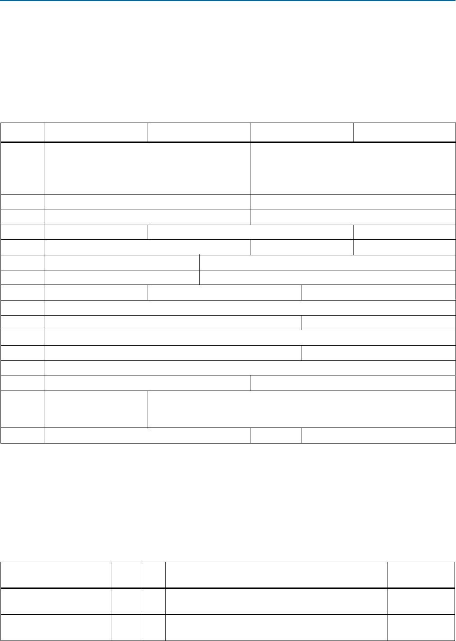
Configuration Space Register Access
The
tl_cfg_ctl
signal is a multiplexed bus that contains the contents of
Configuration Space registers as shown in Table 7–10. Information stored in the
Configuration Space is accessed in round robin order where
tl_cfg_add
indicates
which register is being accessed. Table 7–12 shows the layout of configuration
information that is multiplexed on
tl_cfg_ctl
.
Table 7–13 describes the Configuration Space registers referred to in Table 7–10 and
Table 7–12.
Table 7–12. Multiplexed Configuration Register Information Available on tl_cfg_ctl
(1)
Index 31:24 23:16 15:8 7:0
0
cfg_dev_ctrl_func<n>[15:0]
cfg_dev_ctrl2[15:0]
cfg_dev_ctrl[14:12]=
Max Read Req Size
(2)
cfg_dev_ctrl[7:5]=
Max Payload
(2)
1
16’h0000 cfg_slot_ctrl[15:0]
2
cfg_link_ctrl[15:0] cfg_link_ctrl2[15:0]
3
8’h00 cfg_prm_cmd_func<n>[15:0] cfg_root_ctrl[7:0]
4
cfg_sec_ctrl[15:0] cfg_secbus[7:0] cfg_subbus[7:0]
5
cfg_msi_addr[11:0] cfg_io_bas[19:0]
6
cfg_msi_addr[43:32] cfg_io_lim[19:0]
7
8h’00 cfg_np_bas[11:0] cfg_np_lim[11:0]
8
cfg_pr_bas[31:0]
9
cfg_msi_addr[31:12] cfg_pr_bas[43:32]
A
cfg_pr_lim[31:0]
B
cfg_msi_addr[63:44] cfg_pr_lim[43:32]
C
cfg_pmcsr[31:0]
D
cfg_msixcsr[15:0] cfg_msicsr[15:0]
E
6’h00,
tx_ecrcgen[25],
(3)
rx_ecrccheck[24]
cfg_tcvcmap[23:0]
F
cfg_msi_data[15:0]
3’b000
cfg_busdev[12:0]
Notes to Table 7–12:
(1) Items in blue are only available for Root Ports.
(2) This field is encoded as specified in Section 7.8.4 of the PCI Express Base Specification. (3’b000–3’b101 correspond to 128–4096 bytes).
(3)
rx_ecrccheck
and
tx_ecrcgen
are bit s 24 and 25 of
tl_cfg_ctl
, respectively. (Other bit specifications in this table indicate the bit location
within the Configuration Space register.)
Table 7–13. Configuration Space Register Descriptions (Part 1 of 4)
Register
Width Dir Description
Register
Reference
cfg_dev_ctrl_func<n>
16 O
cfg_dev_ctrl_func<n>[15:0]
is Device Control
register for the PCI Express capability structure.
Table 8–7 on
page 8–4
cfg_dev_ctrl2
16 O
cft_dev_ctrl2[31:16]
is Device Control register 2 for
the PCI Express capability structure.
Table 8–8 on
page 8–4