
User guide
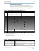
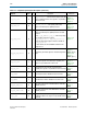


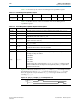
Table Of Contents
- Cyclone V Hard IP for PCI Express User Guide
- Contents
- 1. Datasheet
- 2. Getting Started with the Cyclone V Hard IP for PCI Express
- 3. Getting Started with the Avalon-MM Cyclone Hard IP for PCI Express
- Running Qsys
- Customizing the Cyclone VHard IP for PCI Express IP Core
- Adding the Remaining Components to the Qsys System
- Completing the Connections in Qsys
- Specifying Clocks and Interrupts
- Specifying Exported Interfaces
- Specifying Address Assignments
- Simulating the Example Design
- Simulating the Single DWord Design
- Understanding Channel Placement Guidelines
- Adding Synopsis Design Constraints
- Creating a Quartus II Project
- Compiling the Design
- Programming a Device
- 4. Parameter Settings for the Cyclone V Hard IP for PCI Express
- 5. Parameter Settings for the Avalon-MM Cyclone V Hard IP for PCI Express
- 6. IP Core Architecture
- Key Interfaces
- Protocol Layers
- Multi-Function Support
- PCI Express Avalon-MM Bridge
- Avalon-MM Bridge TLPs
- Avalon-MM-to-PCI Express Write Requests
- Avalon-MM-to-PCI Express Upstream Read Requests
- PCI Express-to-Avalon-MM Read Completions
- PCI Express-to-Avalon-MM Downstream Write Requests
- PCI Express-to-Avalon-MM Downstream Read Requests
- Avalon-MM-to-PCI Express Read Completions
- PCI Express-to-Avalon-MM Address Translation for Endpoints
- Minimizing BAR Sizes and the PCIe Address Space
- Avalon-MM-to-PCI Express Address Translation Algorithm
- Single DWord Completer Endpoint
- 7. IP Core Interfaces
- Cyclone V Hard IP for PCI Express
- Avalon-MM Hard IP for PCI Express
- Physical Layer Interface Signals
- Test Signals
- 8. Register Descriptions
- Configuration Space Register Content
- Altera-Defined Vendor Specific Extended Capability (VSEC)
- PCI Express Avalon-MM Bridge Control Register Access Content
- Avalon-MM to PCI Express Interrupt Registers
- PCI Express Mailbox Registers
- Avalon-MM-to-PCI Express Address Translation Table
- Root Port TLP Data Registers
- Programming Model for Avalon-MM Root Port
- PCI Express to Avalon-MM Interrupt Status and Enable Registers for Root Ports
- PCI Express to Avalon-MM Interrupt Status and Enable Registers for Endpoints
- Avalon-MM Mailbox Registers
- Correspondence between Configuration Space Registers and the PCIe Spec 2.1
- 9. Reset and Clocks
- 10. Transaction Layer Protocol (TLP) Details
- 11. Interrupts
- Interrupts for Endpoints Using the Avalon-ST Application Interface
- Interrupts for Root Ports Using the Avalon-ST Interface to the Application Layer
- Interrupts for Endpoints Using the Avalon-MM Interface to the Application Layer
- Interrupts for End Points Using the Avalon-MM Interface with Multiple MSI/MSI-X Support
- 12. Optional Features
- 13. Flow Control
- 14. Error Handling
- 15. Transceiver PHY IP Reconfiguration
- 16. SDC Timing Constraints
- 17. Testbench and Design Example
- Endpoint Testbench
- Root Port Testbench
- Chaining DMA Design Examples
- Test Driver Module
- Root Port Design Example
- Root Port BFM
- BFM Procedures and Functions
- 18. Debugging
- A. Transaction Layer Packet (TLP) Header Formats
- Additional Information

Chapter 7: IP Core Interfaces 7–33
Cyclone V Hard IP for PCI Express
December 2013 Altera Corporation Cyclone V Hard IP for PCI Express
User Guide
Table 7–11 describes the bits of the
tl_cfg_sts
bus for all eight functions. Refer to
Table 7–12 on page 7–35 for the layout of the configuration control and status
information.
Table 7–11. Mapping Between tl_cfg_sts and Configuration Space Registers (Part 1 of 2)
tl_cfg_sts Configuration Space Register Description
[62:59] Func1
[72:69] Func2
[82:79] Func3
[92:89] Func4
[102:99] Func5
[112:109] Func6
[122:119] Func7
Device Status Reg[3:0]
Records the following errors:
■ Bit 3: unsupported request
■ Bit 2: fatal error
■ Bit 1: non-fatal error
■ Bit 0: correctable error
[58:54] Func1
[68:64] Func2
[78:74] Func3
[88:84] Func4
[98:94] Func5
[108:104] Func6
[118:114] Func7
Link Status Reg[15:11]
Link status bits as follows:
■ Bit 15: link autonomous bandwidth status
■ Bit 14: link bandwidth management status
■ Bit 13: Data Link Layer link active
■ Bit 12: slot clock configuration
■ Bit 11: link training
[53] Func1
[63] Func2
[73] Func3
[83] Func4
[93] Func5
[103] Func6
[113] Func7
Secondary Status Register[8] 6th primary command status error bit. Master data parity error.
[52:49] Device Status Register[3:0]
Records the following errors:
■ Bit 3: unsupported request detected
■ Bit 2: fatal error detected
■ Bit 1: non-fatal error detected
■ Bit 0: correctable error detected
[48] Slot Status Register[8] Data Link Layer state changed
[47] Slot Status Register[4]
Command completed. (The hot plug controller completed a
command.)
[46:31] Link Status Register[15:0]
Records the following link status information:
■ Bit 15: link autonomous bandwidth status
■ Bit 14: link bandwidth management status
■ Bit 13: Data Link Layer link active
■ Bit 12: Slot clock configuration
■ Bit 11: Link Training
■ Bit 10: Undefined
■ Bits[9:4]: Negotiated Link Width
■ Bits[3:0] Link Speed
[30] Link Status 2 Register[0] Current de-emphasis level.