
User guide

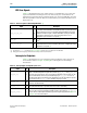

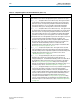

Table Of Contents
- Cyclone V Hard IP for PCI Express User Guide
- Contents
- 1. Datasheet
- 2. Getting Started with the Cyclone V Hard IP for PCI Express
- 3. Getting Started with the Avalon-MM Cyclone Hard IP for PCI Express
- Running Qsys
- Customizing the Cyclone VHard IP for PCI Express IP Core
- Adding the Remaining Components to the Qsys System
- Completing the Connections in Qsys
- Specifying Clocks and Interrupts
- Specifying Exported Interfaces
- Specifying Address Assignments
- Simulating the Example Design
- Simulating the Single DWord Design
- Understanding Channel Placement Guidelines
- Adding Synopsis Design Constraints
- Creating a Quartus II Project
- Compiling the Design
- Programming a Device
- 4. Parameter Settings for the Cyclone V Hard IP for PCI Express
- 5. Parameter Settings for the Avalon-MM Cyclone V Hard IP for PCI Express
- 6. IP Core Architecture
- Key Interfaces
- Protocol Layers
- Multi-Function Support
- PCI Express Avalon-MM Bridge
- Avalon-MM Bridge TLPs
- Avalon-MM-to-PCI Express Write Requests
- Avalon-MM-to-PCI Express Upstream Read Requests
- PCI Express-to-Avalon-MM Read Completions
- PCI Express-to-Avalon-MM Downstream Write Requests
- PCI Express-to-Avalon-MM Downstream Read Requests
- Avalon-MM-to-PCI Express Read Completions
- PCI Express-to-Avalon-MM Address Translation for Endpoints
- Minimizing BAR Sizes and the PCIe Address Space
- Avalon-MM-to-PCI Express Address Translation Algorithm
- Single DWord Completer Endpoint
- 7. IP Core Interfaces
- Cyclone V Hard IP for PCI Express
- Avalon-MM Hard IP for PCI Express
- Physical Layer Interface Signals
- Test Signals
- 8. Register Descriptions
- Configuration Space Register Content
- Altera-Defined Vendor Specific Extended Capability (VSEC)
- PCI Express Avalon-MM Bridge Control Register Access Content
- Avalon-MM to PCI Express Interrupt Registers
- PCI Express Mailbox Registers
- Avalon-MM-to-PCI Express Address Translation Table
- Root Port TLP Data Registers
- Programming Model for Avalon-MM Root Port
- PCI Express to Avalon-MM Interrupt Status and Enable Registers for Root Ports
- PCI Express to Avalon-MM Interrupt Status and Enable Registers for Endpoints
- Avalon-MM Mailbox Registers
- Correspondence between Configuration Space Registers and the PCIe Spec 2.1
- 9. Reset and Clocks
- 10. Transaction Layer Protocol (TLP) Details
- 11. Interrupts
- Interrupts for Endpoints Using the Avalon-ST Application Interface
- Interrupts for Root Ports Using the Avalon-ST Interface to the Application Layer
- Interrupts for Endpoints Using the Avalon-MM Interface to the Application Layer
- Interrupts for End Points Using the Avalon-MM Interface with Multiple MSI/MSI-X Support
- 12. Optional Features
- 13. Flow Control
- 14. Error Handling
- 15. Transceiver PHY IP Reconfiguration
- 16. SDC Timing Constraints
- 17. Testbench and Design Example
- Endpoint Testbench
- Root Port Testbench
- Chaining DMA Design Examples
- Test Driver Module
- Root Port Design Example
- Root Port BFM
- BFM Procedures and Functions
- 18. Debugging
- A. Transaction Layer Packet (TLP) Header Formats
- Additional Information

7–28 Chapter 7: IP Core Interfaces
Cyclone V Hard IP for PCI Express
Cyclone V Hard IP for PCI Express December 2013 Altera Corporation
User Guide
ECC Error Signals
Table 7–7 describes the ECC error signals. When a correctable ECC error occurs, the
Cyclone V Hard IP for PCI Express recovers without any loss of information. No
Application Layer intervention is required. In the case of uncorrectable ECC error, the
data in retry buffer is cleared. Altera recommends that you reset the Hard IP for PCI
Express IP Core.
Interrupts for Endpoints
Table 7–8 describes the IP core’s interrupt signals for Endpoints. These signals are
level sensitive. Refer to Chapter 11, Interrupts for descriptions of all interrupt
mechanisms.
Table 7–7. ECC Error Signals for Hard IP Implementation
(1)
Signal I/O Description
derr_cor_ext_rcv0
O
Indicates a corrected error in the RX buffer. This signal is for debug only. It
is not valid until the RX buffer is filled with data. This is a pulse, not a level,
signal. Internally, the pulse is generated with the 250 MHz clock. A pulse
extender extends the signal so that the FPGA fabric running at 125 MHz
can capture it. Because the error was corrected by the IP core, no
Application Layer intervention is required.
(2)
derr_rpl
O
Indicates an uncorrectable error in the retry buffer. This signal is for debug
only.
(2)
derr_cor_ext_rpl
O
Indicates a corrected ECC error in the retry buffer. This signal is for debug
only. Because the error was corrected by the IP core, no Application Layer
intervention is required.
(2)
Note to Table 7–7:
(1) The Avalon-ST
rx_st_err
described in Table 7–3 on page 7–6 indicates an uncorrectable error in the RX buffer.
(2) Debug signals are not rigorously verified and should only be used to observe behavior.
Table 7–8. Interrupt Signals for Endpoints (Part 1 of 2)
Signal I/O Description
app_msi_req
I
Application Layer MSI request. Assertion causes an MSI posted write TLP to be generated
based on the MSI configuration register values and the tl_
app_msi_tc
and
app_msi_num
input ports. In Root Port mode, the core generates an MSI TLP to the Root Port over the
Avalon-ST RX interface. In this case, the header bit[127] of
rx_st_data
is set to 1 to
indicate that the TLP being forwarded to the Application Layer was generated in response
to an assertion of the
app_msi_req
pin; otherwise, bit[127] is set to 0.
app_msi_ack
O
Application Layer MSI acknowledge. This signal acknowledges the Application Layer's
request for an MSI interrupt.
app_msi_tc[2:0]
I
Application Layer MSI traffic class. This signal indicates the traffic class used to send the
MSI (unlike INTX interrupts, any traffic class can be used to send MSIs).
app_msi_num[4:0]
I
MSI number of the Application Layer. This signal provides the low order message data
bits to be sent in the message data field of MSI messages requested by tl_
app_msi_req
.
Only bits that are enabled by the MSI Message Control register apply. Refer to Table 7–14
on page 7–38 for more information.