
User guide
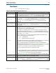
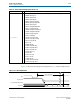


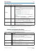

Table Of Contents
- Cyclone V Hard IP for PCI Express User Guide
- Contents
- 1. Datasheet
- 2. Getting Started with the Cyclone V Hard IP for PCI Express
- 3. Getting Started with the Avalon-MM Cyclone Hard IP for PCI Express
- Running Qsys
- Customizing the Cyclone VHard IP for PCI Express IP Core
- Adding the Remaining Components to the Qsys System
- Completing the Connections in Qsys
- Specifying Clocks and Interrupts
- Specifying Exported Interfaces
- Specifying Address Assignments
- Simulating the Example Design
- Simulating the Single DWord Design
- Understanding Channel Placement Guidelines
- Adding Synopsis Design Constraints
- Creating a Quartus II Project
- Compiling the Design
- Programming a Device
- 4. Parameter Settings for the Cyclone V Hard IP for PCI Express
- 5. Parameter Settings for the Avalon-MM Cyclone V Hard IP for PCI Express
- 6. IP Core Architecture
- Key Interfaces
- Protocol Layers
- Multi-Function Support
- PCI Express Avalon-MM Bridge
- Avalon-MM Bridge TLPs
- Avalon-MM-to-PCI Express Write Requests
- Avalon-MM-to-PCI Express Upstream Read Requests
- PCI Express-to-Avalon-MM Read Completions
- PCI Express-to-Avalon-MM Downstream Write Requests
- PCI Express-to-Avalon-MM Downstream Read Requests
- Avalon-MM-to-PCI Express Read Completions
- PCI Express-to-Avalon-MM Address Translation for Endpoints
- Minimizing BAR Sizes and the PCIe Address Space
- Avalon-MM-to-PCI Express Address Translation Algorithm
- Single DWord Completer Endpoint
- 7. IP Core Interfaces
- Cyclone V Hard IP for PCI Express
- Avalon-MM Hard IP for PCI Express
- Physical Layer Interface Signals
- Test Signals
- 8. Register Descriptions
- Configuration Space Register Content
- Altera-Defined Vendor Specific Extended Capability (VSEC)
- PCI Express Avalon-MM Bridge Control Register Access Content
- Avalon-MM to PCI Express Interrupt Registers
- PCI Express Mailbox Registers
- Avalon-MM-to-PCI Express Address Translation Table
- Root Port TLP Data Registers
- Programming Model for Avalon-MM Root Port
- PCI Express to Avalon-MM Interrupt Status and Enable Registers for Root Ports
- PCI Express to Avalon-MM Interrupt Status and Enable Registers for Endpoints
- Avalon-MM Mailbox Registers
- Correspondence between Configuration Space Registers and the PCIe Spec 2.1
- 9. Reset and Clocks
- 10. Transaction Layer Protocol (TLP) Details
- 11. Interrupts
- Interrupts for Endpoints Using the Avalon-ST Application Interface
- Interrupts for Root Ports Using the Avalon-ST Interface to the Application Layer
- Interrupts for Endpoints Using the Avalon-MM Interface to the Application Layer
- Interrupts for End Points Using the Avalon-MM Interface with Multiple MSI/MSI-X Support
- 12. Optional Features
- 13. Flow Control
- 14. Error Handling
- 15. Transceiver PHY IP Reconfiguration
- 16. SDC Timing Constraints
- 17. Testbench and Design Example
- Endpoint Testbench
- Root Port Testbench
- Chaining DMA Design Examples
- Test Driver Module
- Root Port Design Example
- Root Port BFM
- BFM Procedures and Functions
- 18. Debugging
- A. Transaction Layer Packet (TLP) Header Formats
- Additional Information

7–26 Chapter 7: IP Core Interfaces
Cyclone V Hard IP for PCI Express
Cyclone V Hard IP for PCI Express December 2013 Altera Corporation
User Guide
pld_clk_inuse
O
When asserted, indicates that the Hard IP Transaction Layer is using the
pld_clk
as its
clock and is ready for operation with the Application Layer. For reliable operation, hold the
Application Layer in reset until
pld_clk_inuse
is asserted.
Do not drive data input to the Hard IP before
pld_clk_inuse
is asserted.
pld_clk_inuse
and
pld_core_ready
are typically used as handshaking signals after programming the
FPGA fabric with CvP. These handshaking signals ensure a reliable Hard IP clock switchover
from an internal clock used during the CvP operation to the
pld_clk
Hard IP input clock.
dlup_exit
O
This signal is active for one
pld_clk
cycle when the IP core exits the DLCMSM DL_Up state,
indicating that the Data Link Layer has lost communication with the other end of the PCIe
link and left the Up state. This signal should cause the Application Layer to assert a global
reset. This signal is active low and otherwise remains high.
ev128ns
O Asserted every 128 ns to create a time base aligned activity.
ev1us
O Asserted every 1 µs to create a time base aligned activity.
hotrst_exit
O
Hot reset exit. This signal is asserted for 1 clock cycle when the LTSSM exits the hot reset
state. This signal should cause the Application Layer to assert a global reset to its logic. This
signal is active low and otherwise remains high.
l2_exit
O
L2 exit. This signal is active low and otherwise remains high. It is asserted for one cycle
(changing value from 1 to 0 and back to 1) after the LTSSM transitions from l2_idl to detect.
current_speed
O
Indicates the current speed of the PCIe link. The following encodings are defined:
■ 2b’00: Reserved
■ 2b’01: Gen1
■ 2’b10: Gen2
■ 2’b11: Gen3
Table 7–6. Reset and Link Training Signals (Part 2 of 3)
Signal I/O Description