Cyclone V Hard IP for PCI Express User Guide Cyclone V Hard IP for PCI Express User Guide 101 Innovation Drive San Jose, CA 95134 www.altera.com 4UG-01110-1.5 Document last updated for Altera Complete Design Suite version: Document publication date: 13.
© 2013 Altera Corporation. All rights reserved. ALTERA, ARRIA, CYCLONE, HARDCOPY, MAX, MEGACORE, NIOS, QUARTUS and STRATIX words and logos are trademarks of Altera Corporation and registered in the U.S. Patent and Trademark Office and in other countries. All other words and logos identified as trademarks or service marks are the property of their respective holders as described at www.altera.com/common/legal.html.
Contents Chapter 1. Datasheet Features . . . . . . . . . . . . . . . . . . . . . . . . . . . . . . . . . . . . . . . . . . . . . . . . . . . . . . . . . . . . . . . . . . . . . . . . . . . . . . . . 1–1 Release Information . . . . . . . . . . . . . . . . . . . . . . . . . . . . . . . . . . . . . . . . . . . . . . . . . . . . . . . . . . . . . . . . . . . . . 1–4 Device Family Support . . . . . . . . . . . . . . . . . . . . . . . . . . . . . . . . . . . . . . . . . . . . . . . . . . . . . . . . . . . . . .
Parameters Defined Separately for All Port Functions . . . . . . . . . . . . . . . . . . . . . . . . . . . . . . . . . . . . . . 4–7 Base Address Registers for Function . . . . . . . . . . . . . . . . . . . . . . . . . . . . . . . . . . . . . . . . . . . . . . 4–8 Base and Limit Registers for Root Port Func . . . . . . . . . . . . . . . . . . . . . . . . . . . . . . . . . . . . . . . . 4–8 Device ID Registers for Function . . . . . . . . . . . . . . . . . . . . . . . . . . . . . . . . . . . . .
Avalon-ST Packets to PCI Express TLPs . . . . . . . . . . . . . . . . . . . . . . . . . . . . . . . . . . . . . . . . . . . . . . . . . . 7–5 Avalon-ST RX Interface . . . . . . . . . . . . . . . . . . . . . . . . . . . . . . . . . . . . . . . . . . . . . . . . . . . . . . . . . . . . . . . . 7–6 Data Alignment and Timing for the 64-Bit Avalon-ST RX Interface . . . . . . . . . . . . . . . . . . . . . . . . 7–9 Data Alignment and Timing for the 128-Bit Avalon-ST RX Interface . . . . . . . . . . . . . . . . .
pld_clk . . . . . . . . . . . . . . . . . . . . . . . . . . . . . . . . . . . . . . . . . . . . . . . . . . . . . . . . . . . . . . . . . . . . . . . . . . . . . . 9–6 Transceiver Clock Signals . . . . . . . . . . . . . . . . . . . . . . . . . . . . . . . . . . . . . . . . . . . . . . . . . . . . . . . . . . . . . . 9–6 Chapter 10. Transaction Layer Protocol (TLP) Details Supported Message Types . . . . . . . . . . . . . . . . . . . . . . . . . . . . . . . . . . . . . . . . . . . . . . . . . . . . . . . .
DMA Read Cycles . . . . . . . . . . . . . . . . . . . . . . . . . . . . . . . . . . . . . . . . . . . . . . . . . . . . . . . . . . . . . . . . 17–17 Root Port Design Example . . . . . . . . . . . . . . . . . . . . . . . . . . . . . . . . . . . . . . . . . . . . . . . . . . . . . . . . . . . . . . 17–18 Root Port BFM . . . . . . . . . . . . . . . . . . . . . . . . . . . . . . . . . . . . . . . . . . . . . . . . . . . . . . . . . . . . . . . . . . . . . . . . 17–20 BFM Memory Map . . . . . . . . . . . . . .
rc_mempoll Procedure . . . . . . . . . . . . . . . . . . . . . . . . . . . . . . . . . . . . . . . . . . . . . . . . . . . . . . . . . . . . 17–46 msi_poll Procedure . . . . . . . . . . . . . . . . . . . . . . . . . . . . . . . . . . . . . . . . . . . . . . . . . . . . . . . . . . . . . . . 17–47 dma_set_msi Procedure . . . . . . . . . . . . . . . . . . . . . . . . . . . . . . . . . . . . . . . . . . . . . . . . . . . . . . . . . . . 17–47 find_mem_bar Procedure . . . . . . . . . . . . . . . . . . . . . . .
1. Datasheet December 2013 UG-01110-1.5 This document describes the Altera® Cyclone® Hard IP for PCI Express®. PCI Express is a high-performance interconnect protocol for use in a variety of applications including network adapters, storage area networks, embedded controllers, graphic accelerator boards, and audio-video products. The PCI Express protocol is software backwards-compatible with the earlier PCI and PCI-X protocols, but is significantly different from its predecessors.
1–2 Chapter 1: Datasheet Features ■ Qsys support using the Avalon Memory-Mapped (Avalon-MM) with a 64- or 128-bit interface to the Application Layer ■ Extended credit allocation settings to better optimize the RX buffer space based on application type. ■ Qsys example designs demonstrating parameterization, design modules and connectivity. ■ Optional end-to-end cyclic redundancy code (ECRC) generation and checking and advanced error reporting (AER) for high reliability applications.
Chapter 1: Datasheet Features 1–3 Table 1–1.
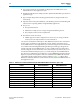
1–4 Chapter 1: Datasheet Release Information Release Information Table 1–3 provides information about this release of the PCI Express Compiler. Table 1–2. PCI Express Compiler Release Information Item Description Version 13.1 Release Date December 2013 Ordering Codes Product IDs Vendor ID No ordering code is required There are no encrypted files for the Cyclone V Hard IP for PCI Express. The Product ID and Vendor ID are not required because this IP core does not require a license.
Chapter 1: Datasheet Debug Features 1–5 Optimized for Altera devices, the Cyclone V Hard IP for PCI Express supports all memory, I/O, configuration, and message transactions. It has a highly optimized Application Layer interface to achieve maximum effective throughput. You can customize the Hard IP to meet your design requirements using either the MegaWizard Plug-In Manager or the Qsys design flow. Figure 1–1 shows a PCI Express link between two Cyclone V FPGAs.
1–6 Chapter 1: Datasheet IP Core Verification IP Core Verification To ensure compliance with the PCI Express specification, Altera performs extensive validation of the Cyclone V Hard IP Core for PCI Express. The simulation environment uses multiple testbenches that consist of industry-standard BFMs driving the PCI Express link interface. A custom BFM connects to the application-side interface.
Chapter 1: Datasheet Recommended Speed Grades 1–7 Soft calibration of the transceiver module requires additional logic. The amount of logic required depends upon the configuration. Recommended Speed Grades Table 1–6 lists the recommended speed grades for the supported link widths and Application Layer clock frequencies. The speed grades listed are the only speed grades that close timing. Altera recommends setting the Quartus II Analysis & Synthesis Settings Optimization Technique to Speed.
1–8 Cyclone V Hard IP for PCI Express User Guide Chapter 1: Datasheet Recommended Speed Grades December 2013 Altera Corporation
2. Getting Started with the Cyclone V Hard IP for PCI Express December 2013 UG-01110-1.5 This section provides step-by-step instructions to help you quickly customize, simulate, and compile the Cyclone V Hard IP for PCI Express using either the MegaWizard Plug-In Manager or Qsys design flow. When you install the Quartus II software you also install the IP Library.
2–2 Chapter 2: Getting Started with the Cyclone V Hard IP for PCI Express The Cyclone V Hard IP for PCI Express offers exactly the same feature set in both the MegaWizard and Qsys design flows. Consequently, your choice of design flow depends on whether you want to integrate the Cyclone V Hard IP for PCI Express using RTL instantiation or using Qsys, which is a system integration tool available in the Quartus II software.
Chapter 2: Getting Started with the Cyclone V Hard IP for PCI Express MegaWizard Plug-In Manager Design Flow 2–3 MegaWizard Plug-In Manager Design Flow This section guides you through the steps necessary to customize the Cyclone V Hard IP for PCI Express and run the example testbench, starting with the creation of a Quartus II project. Follow these steps to copy the example design files and create a Quartus II project. 1.
2–4 Chapter 2: Getting Started with the Cyclone V Hard IP for PCI Express Customizing the Endpoint in the MegaWizard Plug-In Manager Design Flow 1. On the Tools menu, click MegaWizard Plug-In Manager. The MegaWizard Plug-In Manager appears. 2. Select Create a new custom megafunction variation and click Next. 3. In Which device family will you be using? Select the Cyclone V device family. 4.
Chapter 2: Getting Started with the Cyclone V Hard IP for PCI Express Customizing the Endpoint in the MegaWizard Plug-In Manager Design Flow 2–5 Table 2–2. Device Parameter Value Completion timeout range ABCD Implement completion timeout disable On 10. On the Error Reporting tab, leave all options off. 11. Specify the Link settings listed in Table 2–7. Table 2–3. Link Tab Parameter Value Link port number 1 Slot clock configuration On 12.
2–6 Chapter 2: Getting Started with the Cyclone V Hard IP for PCI Express Customizing the Endpoint in the MegaWizard Plug-In Manager Design Flow Table 2–6. Device ID Registers for Func0 Device ID 0x00000001 0x0000E001 Revision ID 0x00000001 0x00000001 Class Code 0x00000000 0x00FF0000 Subsystem Vendor ID 0x00000000 0x00001172 Subsystem Device ID 0x00000000 0x0000E001 19. On the Func 0 Device tab, under PCI Express/PCI Capabilities for Func 0 turn Function Level Reset (FLR) Off. 20.
Chapter 2: Getting Started with the Cyclone V Hard IP for PCI Express Customizing the Endpoint in the MegaWizard Plug-In Manager Design Flow 2–7 2. Navigate to the Qsys system in the altera_pcie__hip_ast subdirectory. 3. Click pcie_de_gen1_x4_ast64.qsys to bring up the Qsys design. Figure 2–3 illustrates this Qsys system. Figure 2–3.
2–8 Chapter 2: Getting Started with the Cyclone V Hard IP for PCI Express Customizing the Endpoint in the MegaWizard Plug-In Manager Design Flow 4. To display the parameters of the APPS component shown in Figure 2–3, click on it and then select Edit from the right-mouse menu Figure 2–4. illustrates this component.
Chapter 2: Getting Started with the Cyclone V Hard IP for PCI Express Qsys Design Flow 2–9 Qsys Design Flow This section guides you through the steps necessary to customize the Cyclone V Hard IP for PCI Express and run the example testbench in Qsys. Reviewing the Qsys Example Design for PCIe For this example, copy the Gen1 x4 Endpoint example design from installation directory: /ip/altera/altera_pcie/altera_pcie_hip_ast_ed/example_design / directory to a working directory.
2–10 Chapter 2: Getting Started with the Cyclone V Hard IP for PCI Express Qsys Design Flow ■ pcie_reconfig_driver_0—This Avalon-MM master drives the Transceiver Reconfiguration Controller. The pcie_reconfig_driver_0 is implemented in clear text that you can modify if your design requires different reconfiguration functions.
Chapter 2: Getting Started with the Cyclone V Hard IP for PCI Express Qsys Design Flow 2–11 Understanding the Files Generated Table 2–10 provides an overview of the files and directories Qsys generates. Table 2–10. Qsys Generation Output Files Directory Description // synthesis includes the top-level HDL file for the Hard I for PCI Express and the .
2–12 Chapter 2: Getting Started with the Cyclone V Hard IP for PCI Express Qsys Design Flow ■ Root Port to Endpoint memory reads and writes Example 2–1. Excerpts from Transcript of Successful Simulation Run Time: 56000 Instance: top_chaining_testbench.ep.epmap.pll_250mhz_to_500mhz. # Time: 0 Instance: pcie_de_gen1_x8_ast128_tb.dut_pcie_tb.genblk1.genblk1.altpcietb_bfm_top_rp.rp.rp.nl00O 0i.Cycloneii_pll.
Chapter 2: Getting Started with the Cyclone V Hard IP for PCI Express Qsys Design Flow 2–13 Example 2–1. Excerpts from Transcript of Successful Simulation Run (continued) # INFO: 8973 ns RP LTSSM State: CONFIG.LANENUM.
2–14 Chapter 2: Getting Started with the Cyclone V Hard IP for PCI Express Qsys Design Flow Example 2-1Excerpts from Transcript of Successful Simulation Run (continued) # INFO: 96005 ns multi_message_enable = 0x0002 # INFO: 96005 ns msi_number = 0001 # INFO: 96005 ns msi_traffic_class = 0000 # INFO: 96005 ns --------# INFO: 96005 ns TASK:dma_set_header WRITE # INFO: 96005 ns Writing Descriptor header # INFO: 96045 ns data content of the DT header # INFO: 96045 ns # INFO: 96045 ns Shared Memory Data Displa
Chapter 2: Getting Started with the Cyclone V Hard IP for PCI Express Compiling the Design in the Qsys Design Flow 2–15 Compiling the Design in the MegaWizard Plug-In Manager Design Flow Before compiling the complete example design in the Quartus II software, you must add the example design files that you generated in Qsys to your Quartus II project. The Quartus II IP File (.qip) lists all files necessary to compile the project. Follow these steps to add the Quartus II IP File (.qip) to the project: 1.
2–16 Chapter 2: Getting Started with the Cyclone V Hard IP for PCI Express Compiling the Design in the Qsys Design Flow 2. Click the browse button next the File name box and browse to the gen1_x4_example_design/altera_pcie__ip_ast/pcie_de_gen1_x4_ast64/ synthesis/ directory. 3. On the Quartus II File menu, click New, then New Quartus II Project, then OK. 4. Click Next in the New Project Wizard: Introduction (The introduction does not appear if you previously turned it off.) 5.
Chapter 2: Getting Started with the Cyclone V Hard IP for PCI Express Compiling the Design in the Qsys Design Flow 2–17 14. Add the Synopsys Design Constraint (SDC) shown inExample 2–3, to the top-level design file for your Quartus II project. Example 2–3.
2–18 Chapter 2: Getting Started with the Cyclone V Hard IP for PCI Express Modifying the Example Design Modifying the Example Design To use this example design as the basis of your own design, replace the Chaining DMA Example shown in Figure 2–6 with your own Application Layer design. Then modify the Root Port BFM driver to generate the transactions needed to test your Application Layer. . Figure 2–6.
3. Getting Started with the Avalon-MM Cyclone Hard IP for PCI Express December 2013 UG-01110-1.5 This Qsys design example provides detailed step-by-step instructions to generate a Qsys system. When you install the Quartus II software you also install the IP Library. This installation includes design examples for the Avalon-MM Cyclone Hard IP for PCI Express in the /ip/altera/altera_pcie/altera_pcie_cv_hip_avmm/ example_designs/ directory.
3–2 Chapter 3: Getting Started with the Avalon-MM Cyclone Hard IP for PCI Express Running Qsys As Figure 3–1 illustrates, the design example transfers data between an on-chip memory buffer located on the Avalon-MM side and a PCI Express memory buffer located on the root complex side. The data transfer uses the DMA component which is programmed by the PCI Express software application running on the Root Complex processor.
Chapter 3: Getting Started with the Avalon-MM Cyclone Hard IP for PCI Express Customizing the Cyclone VHard IP for PCI Express IP Core 3–3 Customizing the Cyclone VHard IP for PCI Express IP Core The parameter editor uses bold headings to divide the parameters into separate sections. You can use the scroll bar on the right to view parameters that are not initially visible. Follow these steps to parameterize the Hard IP for PCI Express IP core: 1.
3–4 Chapter 3: Getting Started with the Avalon-MM Cyclone Hard IP for PCI Express Customizing the Cyclone VHard IP for PCI Express IP Core Table 3–4. Device Identification Registers (Part 2 of 2) Parameter Value Altera Value Revision ID 0x00000001 0x00000001 Class Code 0x00000000 0x00FF0000 Subsystem Vendor ID 0x00000000 0x00001172 Subsystem Device ID 0x00000000 0x0000E001 4. Under the PCI Express and PCI Capabilities heading, specify the settings in Table 3–5. Table 3–5.
Chapter 3: Getting Started with the Avalon-MM Cyclone Hard IP for PCI Express Adding the Remaining Components to the Qsys System 3–5 5. Under the Avalon-MM System Settings heading, specify the settings in Table 3–6. Table 3–6.
3–6 Chapter 3: Getting Started with the Avalon-MM Cyclone Hard IP for PCI Express Adding the Remaining Components to the Qsys System 3. In the DMA Controller parameter editor, specify the parameters and conditions listed in the following table. Table 3–8.
Chapter 3: Getting Started with the Avalon-MM Cyclone Hard IP for PCI Express Adding the Remaining Components to the Qsys System 3–7 Table 3–9. On-Chip Memory Parameters (Part 2 of 2) Parameter Value Enable In-System Memory Content Editor feature D Turn off this option Instance ID Not required 7. Click Finish. 8. The On-chip memory component is added to your Qsys system. 9. On the File menu, click Save and type the file name ep_g1x4.qsys.
3–8 Chapter 3: Getting Started with the Avalon-MM Cyclone Hard IP for PCI Express Completing the Connections in Qsys 12. Click Finish. 13. The Transceiver Reconfiguration Controller is added to your Qsys system. f For more information about the Transceiver Reconfiguration Controller, refer to the Transceiver Reconfiguration Controller chapter in the Altera Transceiver PHY IP Core User Guide.
Chapter 3: Getting Started with the Avalon-MM Cyclone Hard IP for PCI Express Specifying Clocks and Interrupts 3–9 Table 3–11.
3–10 Chapter 3: Getting Started with the Avalon-MM Cyclone Hard IP for PCI Express Specifying Address Assignments Specifying Address Assignments Qsys requires that you resolve the base addresses of all Avalon-MM slave interfaces in the Qsys system. You can either use the auto-assign feature, or specify the base addresses manually. To use the auto-assign feature, on the System menu, click Assign Base Addresses. In the design example, you assign the base addresses manually.
Chapter 3: Getting Started with the Avalon-MM Cyclone Hard IP for PCI Express Simulating the Example Design 3–11 4. After Qsys reports Generate Completed in the Generate progress box title, click Close. 5. On the File menu, click Save. and type the file name ep_g1x4.qsys. Table 3–14 lists the directories that are generated in your Quartus II project directory. Table 3–14.
3–12 Chapter 3: Getting Started with the Avalon-MM Cyclone Hard IP for PCI Express Simulating the Example Design f For more information about IP functional simulation models, refer to Simulating Altera Designs in volume 3 of the Quartus II Handbook. Complete the following steps to run the Qsys testbench: 1. In a terminal window, change to the /ep_g1x4/testbench/mentor directory. 2. Start the ModelSim simulator. 3. To run the simulation, type the following commands in a terminal window: a.
Chapter 3: Getting Started with the Avalon-MM Cyclone Hard IP for PCI Express Simulating the Example Design 3–13 ■ Setup of the DMA controller to write the same data back to the Transaction Layer Direct BFM’s shared memory ■ Data comparison and report of any mismatch Example 3–1 shows the transcript from a successful simulation run. Example 3–1. Transcript from ModelSim Simulation of Gen1 x4 Endpoint # 464 ns Completed initial configuration of Root Port. # INFO: 2657 ns EP LTSSM State: DETECT.
3–14 Chapter 3: Getting Started with the Avalon-MM Cyclone Hard IP for PCI Express Simulating the Example Design Example 3–1.
Chapter 3: Getting Started with the Avalon-MM Cyclone Hard IP for PCI Express Simulating the Single DWord Design 3–15 Example 3–1.
3–16 Chapter 3: Getting Started with the Avalon-MM Cyclone Hard IP for PCI Express Adding Synopsis Design Constraints Adding Synopsis Design Constraints Before you can compile your design using the Quartus II software, you must add a few Synopsys Design Constraints (SDC) to your project. Complete the following steps to add these constraints: 1. Browse to /ep_g1x4/synthesis/submodules. 2. Add the constraints shown inExample 3–2 to altera_pci_express.sdc. Example 3–2.
Chapter 3: Getting Started with the Avalon-MM Cyclone Hard IP for PCI Express Compiling the Design 3–17 9. From the Simulation list, select ModelSim®. From the Format list, select the HDL language you intend to use for simulation. 10. Click Next to display the Summary page. 11. Check the Summary page to ensure that you have entered all the information correctly. Compiling the Design Follow these steps to compile your design: 1. On the Quartus II Processing menu, click Start Compilation. 2.
3–18 Cyclone V Hard IP for PCI Express User Guide Chapter 3: Getting Started with the Avalon-MM Cyclone Hard IP for PCI Express Programming a Device December 2013 Altera Corporation
4. Parameter Settings for the Cyclone V Hard IP for PCI Express December 2013 UG-01110-1.5 This chapter describes the parameters which you can set using the MegaWizard Plug-In Manager or Qsys design flow to instantiate a Cyclone V Hard IP for PCI Express IP core. The appearance of the GUI is identical for the two design flows. 1 In the following tables, hexadecimal addresses in green are links to additional information in the “Register Descriptions” chapter.
4–2 Chapter 4: Parameter Settings for the Cyclone V Hard IP for PCI Express System Settings Table 4–1. System Settings for PCI Express (Part 2 of 3) Parameter Value Description Determines the allocation of posted header credits, posted data credits, non-posted header credits, completion header credits, and completion data credits in the 6 KByte RX buffer. The 5 settings allow you to adjust the credit allocation to optimize your system.
Chapter 4: Parameter Settings for the Cyclone V Hard IP for PCI Express Port Functions 4–3 Table 4–1. System Settings for PCI Express (Part 3 of 3) Parameter Value Reference clock frequency 100 MHz 125 MHz Description The PCI Express Base Specification 2.1 requires a 100 MHz 300 ppm reference clock. The 125 MHz reference clock is provided as a convenience for systems that include a 125 MHz clock source. Use 62.5 MHz Application Layer clock On/Off This mode is only available for Gen1 ×1 variants.
4–4 Chapter 4: Parameter Settings for the Cyclone V Hard IP for PCI Express Port Functions Device Table 4–2 describes the shared device parameters. Table 4–2. Capabilities Registers for Function (Part 1 of 2) Parameter Possible Values Default Value Description Device Capabilities Maximum payload size 128 bytes 256 bytes, 512 bytes, 128 bytes Specifies the maximum payload size supported.
Chapter 4: Parameter Settings for the Cyclone V Hard IP for PCI Express Port Functions 4–5 Table 4–2. Capabilities Registers for Function (Part 2 of 2) Possible Values Parameter Default Value Description The following encodings are used to specify the range: Completion timeout range (continued) ■ 0001 Range A ■ 0010 Range B ■ 0011 Ranges A and B ■ 0110 Ranges B and C ■ 0111 Ranges A, B, and C ■ 1110 Ranges B, C and D ■ 1111 Ranges A, B, C, and D All other values are reserved.
4–6 Chapter 4: Parameter Settings for the Cyclone V Hard IP for PCI Express Port Functions Link Table 4–4 describes the Link Capabilities parameters. Table 4–4. Link Capabilities 0x090 Parameter Value 0x01 Link port number Slot clock configuration (default value) On/Off Description Sets the read-only value of the port number field in the Link Capabilities register. This is an 8-bit field which you can specify.
Chapter 4: Parameter Settings for the Cyclone V Hard IP for PCI Express Port Functions 4–7 Table 4–5. Slot Capabilities 0x094 Parameter Value Description Slot power limit 0–255 In combination with the Slot power scale value, specifies the upper limit in watts on power supplied by the slot. Refer to Section 7.8.9 of the PCI Express Base Specification Revision 2.1 for more information. Slot number 0-8191 Specifies the slot number.
4–8 Chapter 4: Parameter Settings for the Cyclone V Hard IP for PCI Express Port Functions 1 When you click on a Func tab, the parameter settings automatically relate to the function currently selected. Base Address Registers for Function Table 4–7 describes the Base Address (BAR) register parameters. Table 4–7.
Chapter 4: Parameter Settings for the Cyclone V Hard IP for PCI Express Port Functions 4–9 Device ID Registers for Function Table 4–9 lists the default values of the read-only Device ID registers. You can use the parameter editor to change the values of these registers. At run time, you can change the values of these registers using the reconfiguration block signals. For more information, refer to “R**Hard IP Reconfiguration Interface ###if_hip_reconfig###” on page 8–52. Table 4–9.
4–10 Chapter 4: Parameter Settings for the Cyclone V Hard IP for PCI Express Port Functions Link Table 4–12 describes the Link Capabilities register parameters. Table 4–11. Link 0x090 Parameter Value Description Data link layer active reporting On/Off Turn On this parameter for a downstream port, if the component supports the optional capability of reporting the DL_Active state of the Data Link Control and Management State Machine.
Chapter 4: Parameter Settings for the Cyclone V Hard IP for PCI Express Port Functions 4–11 MSI-X Table 4–12 describes the MSI-X Capabilities register parameters. Table 4–13. MSI and MSI-X Capabilities 0x068–0x06C Parameter Implement MSI-X Value On/Off Description When On, enables the MSI-X functionality. Bit Range [10:0] System software reads this field to determine the MSI-X Table size , which is encoded as . For example, a returned value of 2047 indicates a table size of 2048.
4–12 Cyclone V Hard IP for PCI Express User Guide Chapter 4: Parameter Settings for the Cyclone V Hard IP for PCI Express Port Functions December 2013 Altera Corporation
5. Parameter Settings for the Avalon-MM Cyclone V Hard IP for PCI Express December 2013 UG-01110-1.5 This chapter describes the parameters which you can set using the Qsys design flow to instantiate an Avalon-MM Cyclone V Hard IP for PCI Express IP core. 1 In the following tables, hexadecimal addresses in green are links to additional information in the “Register Descriptions” chapter. System Settings The first group of settings defines the overall system. Table 5–1 describes these settings. Table 5–1.
5–2 Chapter 5: Parameter Settings for the Avalon-MM Cyclone V Hard IP for PCI Express Base Address Registers Table 5–1. System Settings for PCI Express (Part 2 of 2) Parameter Value RX Buffer credit allocation performance for received requests Description ■ Balanced–This setting allocates approximately half the RX Buffer space to received requests and the other half of the RX Buffer space to received completions.
Chapter 5: Parameter Settings for the Avalon-MM Cyclone V Hard IP for PCI Express Device Identification Registers 5–3 Device Identification Registers Table 5–3 lists the default values of the read-only Device ID registers. You can edit these values in the GUI. At run time, you can change the values of these registers using the reconfiguration block signals. For more information, refer to “R**Hard IP Reconfiguration Interface ###if_hip_reconfig###” on page 8–52. Table 5–3.
5–4 Chapter 5: Parameter Settings for the Avalon-MM Cyclone V Hard IP for PCI Express PCI Express/PCI Capabilities Device Table 5–4 describes the device parameters. 1 Some of these parameters are stored in the Common Configuration Space Header. Text in green are links to these parameters stored in the Common Configuration Space Header. Table 5–4.
Chapter 5: Parameter Settings for the Avalon-MM Cyclone V Hard IP for PCI Express PCI Express/PCI Capabilities 5–5 Table 5–4. Capabilities Registers for Function (Part 2 of 2) Possible Values Parameter Default Value Completion timeout range All other values are reserved. Altera recommends that the completion timeout mechanism expire in no less than 10 ms. (continued) Implement completion timeout disable Description On/Off On 0x0A8 For PCI Express version 2.
5–6 Chapter 5: Parameter Settings for the Avalon-MM Cyclone V Hard IP for PCI Express PCI Express/PCI Capabilities MSI Table 5–7 describes the MSI Capabilities register parameters. Table 5–7. MSI and MSI-X Capabilities –0x05C, Parameter MSI messages requested Cyclone V Hard IP for PCI Express User Guide Value 1, 2, 4, 8, 16 Description Specifies the number of messages the Application Layer can request. Sets the value of the Multiple Message Capable field of the Message Control register, 0x050[31:16].
Chapter 5: Parameter Settings for the Avalon-MM Cyclone V Hard IP for PCI Express PCI Express/PCI Capabilities 5–7 MSI-X Table 5–7 describes the MSI-X Capabilities register parameters. Table 5–8. MSI and MSI-X Capabilities 0x068–0x06C Parameter Implement MSI-X Value On/Off Description When On, enables the MSI-X functionality. Bit Range [10:0] System software reads this field to determine the MSI-X Table size , which is encoded as .
5–8 Chapter 5: Parameter Settings for the Avalon-MM Cyclone V Hard IP for PCI Express PCI Express/PCI Capabilities Power Management Table 5–9 describes the Power Management parameters. Table 5–9. Power Management Parameters Parameter Value Description This design parameter specifies the maximum acceptable latency that the device can tolerate to exit the L0s state for any links between the device and the root complex.
Chapter 5: Parameter Settings for the Avalon-MM Cyclone V Hard IP for PCI Express Avalon Memory-Mapped System Settings 5–9 Avalon Memory-Mapped System Settings Table 5–10 lists the Avalon-MM system parameter registers. Table 5–10. Avalon Memory-Mapped System Settings Parameter Value Avalon-MM data width 64-bit 128-bit Description Specifies the interface width between the PCI Express Transaction Layer and the Application Layer.
5–10 Chapter 5: Parameter Settings for the Avalon-MM Cyclone V Hard IP for PCI Express Avalon to PCIe Address Translation Settings Avalon to PCIe Address Translation Settings Table 5–11 lists the Avalon-MM PCI Express address translation parameter registers. Table 5–11.
6. IP Core Architecture December 2013 UG-01110-1.5 This chapter describes the architecture of the Cyclone V Hard IP for PCI Express. The Cyclone V Hard IP for PCI Express implements the complete PCI Express protocol stack as defined in the PCI Express Base Specification 2.1. The protocol stack includes the following layers: ■ Transaction Layer—The Transaction Layer contains the Configuration Space, the RX and TX channels, the RX buffer, and flow control credits.
6–2 Chapter 6: IP Core Architecture As Figure 6–1 illustrates, an Avalon-ST interface provides access to the Application Layer which can be either 64 or 128 bits. Table 6–1 provides the Application Layer clock frequencies. Table 6–1. Application Layer Clock Frequencies Lanes Gen1 Gen2 ×1 125 MHz @ 64 bits or 62.
Chapter 6: IP Core Architecture Key Interfaces 6–3 Key Interfaces If you select the Cyclone V Hard IP for PCI Express, your design includes an Avalon-ST interface to the Application Layer. If you select the Avalon-MM Cyclone V Hard IP for PCI Express, your design includes an Avalon-MM interface to the Application Layer. The following sections introduce the interfaces shown in Figure 6–2. . Figure 6–2.
6–4 Chapter 6: IP Core Architecture Key Interfaces credits become available. By tracking the credit consumed information and calculating the credits available, the Application Layer can optimize performance by selecting for transmission only the TLPs that have credits available.
Chapter 6: IP Core Architecture Protocol Layers 6–5 Transceiver Reconfiguration The transceiver reconfiguration interface allows you to dynamically reconfigure the values of analog settings in the PMA block of the transceiver. Dynamic reconfiguration is necessary to compensate for process variations. The Altera Transceiver Reconfiguration Controller IP core provides access to these analog settings.
6–6 Chapter 6: IP Core Architecture Protocol Layers Figure 6–3.
Chapter 6: IP Core Architecture Protocol Layers 6–7 2. The Application Layer requests permission to transmit a TLP. The Application Layer must provide the transaction and must be prepared to provide the entire data payload in consecutive cycles. 3. The Transaction Layer verifies that sufficient flow control credits exist and acknowledges or postpones the request. 4. The Transaction Layer forwards the TLP to the Data Link Layer.
6–8 Chapter 6: IP Core Architecture Protocol Layers ■ Management of the retry buffer ■ Link retraining requests in case of error through the Link Training and Status State Machine (LTSSM) of the Physical Layer Figure 6–4 illustrates the architecture of the DLL. Figure 6–4.
Chapter 6: IP Core Architecture Protocol Layers 6–9 ■ Transaction Layer Packet Checker—This block checks the integrity of the received TLP and generates a request for transmission of an ACK/NAK DLLP. ■ TX Arbitration—This block arbitrates transactions, prioritizing in the following order: a. Initialize FC Data Link Layer packet b. ACK/NAK DLLP (high priority) c. Update FC DLLP (high priority) d. PM DLLP e. Retry buffer TLP f. TLP g. Update FC DLLP (low priority) h.
6–10 Chapter 6: IP Core Architecture Protocol Layers Figure 6–5 illustrates the Physical Layer architecture. Figure 6–5. Physical Layer To Data Link Layer To Link MAC Layer PIPE Interface PHY layer Tx+ / Tx- 8B10B Encoder Scrambler Device Transceiver (per Lane) with 2.5 or 5.
Chapter 6: IP Core Architecture Protocol Layers ■ ■ 6–11 LTSSM—This block implements the LTSSM and logic that tracks what is received and transmitted on each lane. ■ For transmission, it interacts with each MAC lane sub-block and with the LTSTX sub-block by asserting both global and per-lane control bits to generate specific Physical Layer packets. ■ On the receive path, it receives the Physical Layer Packets reported by each MAC lane sub-block.
6–12 Chapter 6: IP Core Architecture Multi-Function Support Multi-Function Support The Cyclone V Hard IP for PCI Express supports up to eight functions for Endpoints. You set up the each function under the Port Functions heading in the parameter editor. You can configure Cyclone V devices to include both Native and Legacy Endpoints. Each function replicates the Configuration Space Registers, including logic for Tag Tracking and Error detection.
Chapter 6: IP Core Architecture PCI Express Avalon-MM Bridge ■ 6–13 Control Register Access (CRA) Slave Module—This optional, 32-bit Avalon-MM dynamic addressing slave port provides access to internal control and status registers from upstream PCI Express devices and external Avalon-MM masters. Implementations that use MSI or dynamic address translation require this port.
6–14 Chapter 6: IP Core Architecture Avalon-MM Bridge TLPs The bridge has the following additional characteristics: ■ Type 0 and Type 1 vendor-defined incoming messages are discarded ■ Completion-to-a-flush request is generated, but not propagated to the interconnect fabric For End Points, each PCI Express base address register (BAR) in the Transaction Layer maps to a specific, fixed Avalon-MM address range. You can use separate BARs to map to various Avalon-MM slaves connected to the RX Master port.
Chapter 6: IP Core Architecture Avalon-MM Bridge TLPs ■ 1 6–15 The Avalon-MM byte enables may deassert, but only in the last qword of the burst. To improve PCI Express throughput, Altera recommends using an Avalon-MM burst master without any byte-enable restrictions.
6–16 Chapter 6: IP Core Architecture Avalon-MM Bridge TLPs As an example, Table 6–2 lists the byte enables for 32-bit data. Table 6–2.
Chapter 6: IP Core Architecture Avalon-MM Bridge TLPs 6–17 PCI Express-to-Avalon-MM Address Translation for Endpoints The PCI Express Avalon-MM Bridge translates the system-level physical addresses, typically up to 64 bits, to the significantly smaller addresses used by the Application Layer’s Avalon-MM slave components. You can specify up to six BARs for address translation when you customize your Hard IP for PCI Express as described in “Base Address Registers for Function ” on page 4–8.
6–18 Chapter 6: IP Core Architecture Avalon-MM Bridge TLPs 2. System software programs BAR1:0 to have a base address of 0x00001234 56789000 3. A TLP received with address 0x00001234 56789870 4. The upper 52 bits (0x0000123456789) are used in the BAR matching process, so this request matches. 5. The lower 12 bits, 0x870, are passed through as the Avalon address on the Rxm_BAR0 Avalon-MM Master port. The BAR matching software replaces the upper 20 bits of the address with the Avalon-MM base address.
Chapter 6: IP Core Architecture Avalon-MM Bridge TLPs 6–19 Figure 6–8 illustrates this Qsys system. (Figure 6–8 uses a filter to hide the Conduit interfaces that are not relevant in this discussion.) Figure 6–8. Qsys System for PCI Express with Poor Address Space Utilization Figure 6–9 illustrates the address map for this system. Figure 6–9. Poor Address Map The auto-assigned base addresses result in the following three large BARs: December 2013 ■ BAR0 is 28 bits.
6–20 Chapter 6: IP Core Architecture Avalon-MM Bridge TLPs This design is consuming 1.25GB of PCIe address space when only 276 MBytes are actually required. The solution is to edit the address map to place the base address of each BAR at 0x0000_0000. Figure 6–10 illustrates the optimized address map. Figure 6–10. Optimized Address Map h For more information about changing Qsys addresses using the Qsys address map, refer to Address Map Tab (Qsys) in Quartus II Help.
Chapter 6: IP Core Architecture Avalon-MM Bridge TLPs 6–21 specifies 32-bit or 64-bit PCI Express addressing for the translated address. Refer to Figure 6–12 on page 6–22. The most significant bits of the Avalon-MM address are used by the system interconnect fabric to select the slave port and are not available to the slave. The next most significant bits of the Avalon-MM address index the address translation entry to be used for the translation process of MSB replacement.
6–22 Chapter 6: IP Core Architecture Single DWord Completer Endpoint ■ Sp[1:0]—the space indication for each entry. Figure 6–12.
Chapter 6: IP Core Architecture Single DWord Completer Endpoint 6–23 Figure 6–13 shows Qsys system that includes a completer-only single dword endpoint. Figure 6–13.
6–24 Chapter 6: IP Core Architecture Single DWord Completer Endpoint f For more information about legal combinations of byte enables, refer to Chapter 3, Avalon Memory-Mapped Interfaces in the Avalon Interface Specifications. TX Block The TX block sends completion information to the Avalon-MM Hard IP for PCI Express which sends this information to the root complex. The TX completion block generates a completion packet with Completer Abort (CA) status and no completion data for unsupported requests.
7. IP Core Interfaces December 2013 UG-01110-1.5 This chapter describes the signals that are part of the Cyclone V Hard IP for PCI Express IP core. It describes the top-level signals in the following IP cores: ■ Cyclone V Hard IP for PCI Express ■ Avalon-MM Hard IP for PCI Express Variants using the Avalon-ST interface are available in both the MegaWizard Plug-In Manager and the Qsys design flows. Variants using the Avalon-MM interface are only available in the Qsys design flow.
7–2 Chapter 7: IP Core Interfaces Table 7–1.
Chapter 7: IP Core Interfaces Cyclone V Hard IP for PCI Express 7–3 Figure 7–2 illustrates this option. Figure 7–2.
7–4 Chapter 7: IP Core Interfaces Cyclone V Hard IP for PCI Express Figure 7–3 illustrates the top-level signals in Cyclone V Hard IP for PCI Express IP core. Signal names that include also exist for functions 1 to 7. Figure 7–3.
Chapter 7: IP Core Interfaces Cyclone V Hard IP for PCI Express 7–5 Avalon-ST Packets to PCI Express TLPs The Hard IP for PCI Express IP Core maps Avalon-ST packets to PCI Express TLPs. These mappings apply to all types of TLPs, including posted, non-posted, and completion TLPs. Message TLPs use the mappings shown for four dword headers.
7–6 Chapter 7: IP Core Interfaces Cyclone V Hard IP for PCI Express . Figure 7–4. Qword Alignment PCB Memory 64 bits . . . 0x18 0x10 0x8 Valid Data Valid Data 0x0 Header 1 Addr = 0x4 The PCI Express Base Specification 2.1 states that receivers may optionally check the address translation (AT) bits in byte 2 of the header and flag the received TLP as malformed if AT is not equal to is 2b’00. The Cyclone V Hard IP for PCI Express IP core does not perform this optional check.
Chapter 7: IP Core Interfaces Cyclone V Hard IP for PCI Express 7–7 Table 7–3. 64- or 128-Bit Avalon-ST RX Datapath (Part 2 of 4) Signal Width Dir 1 rx_st_valid O Avalon-ST Type valid Description Clocks rx_st_data into the Application Layer. Deasserts within 2 clocks of rx_st_ready deassertion and reasserts within 2 clocks of rx_st_ready assertion if more data is available to send. rx_st_valid can be deasserted between the rx_st_sop and rx_st_eop even if rx_st_ready is asserted.
7–8 Chapter 7: IP Core Interfaces Cyclone V Hard IP for PCI Express Table 7–3. 64- or 128-Bit Avalon-ST RX Datapath (Part 3 of 4) Signal Width Dir Avalon-ST Type Description The decoded BAR bits for the TLP. Valid for MRd, MWr, IOWR, and IORD TLPs; ignored for the completion or message TLPs. Valid during the cycle in which rx_st_sop is asserted. Figure 7–8 illustrates the timing of this signal for 64-bit data. Figure 7–11 illustrates the timing of this signal for 128-bit data.
Chapter 7: IP Core Interfaces Cyclone V Hard IP for PCI Express 7–9 Table 7–3. 64- or 128-Bit Avalon-ST RX Datapath (Part 4 of 4) Signal Width Dir 8 16 rx_st_be Avalon-ST Type O component specific O component specific Description Byte enables corresponding to the rx_st_data. The byte enable signals only apply to PCI Express TLP payload fields. When using 64-bit Avalon-ST bus, the width of rx_st_be is 8 bits. This signal is optional.
7–10 Chapter 7: IP Core Interfaces Cyclone V Hard IP for PCI Express Figure 7–6 illustrates the mapping of Avalon-ST RX packets to PCI Express TLPs for a three dword header with qword aligned addresses. Note that the byte enables indicate the first byte of data is not valid and the last dword of data has a single valid byte. Figure 7–6.
Chapter 7: IP Core Interfaces Cyclone V Hard IP for PCI Express 7–11 Figure 7–8 shows the mapping of Avalon-ST RX packet to PCI Express TLPs for TLPs for a four dword header with non-qword addresses with a 64-bit bus. Note that the address of the first dword is 0x4. The address of the first enabled byte is 0x6. This example shows one valid word in the first dword, as indicated by the rx_st_be signal. Figure 7–8.
7–12 Chapter 7: IP Core Interfaces Cyclone V Hard IP for PCI Express Figure 7–10 illustrates back-to-back transmission on the 64-bit Avalon-ST RX interface with no idle cycles between the assertion of rx_st_eop and rx_st_sop. Figure 7–10. 64-Bit Avalon-ST Interface Back-to-Back Receive TLPs coreclkout rx_st_data[63:0] C. C. C. C. CCCC008347890. C. C. C. C. C. C. C. C. C. C. C. C. C. C. C. C. C. C. C. C. C. C. C. C. C. C. C. C.
Chapter 7: IP Core Interfaces Cyclone V Hard IP for PCI Express 7–13 Figure 7–12 shows the mapping of 128-bit Avalon-ST RX packets to PCI Express TLPs for TLPs with a 3 dword header and non-qword aligned addresses. In this case, bits[127:96] represent Data0 because address[2] is set. Figure 7–12.
7–14 Chapter 7: IP Core Interfaces Cyclone V Hard IP for PCI Express Figure 7–14 shows the mapping of 128-bit Avalon-ST RX packets to PCI Express TLPs for a four dword header with qword aligned addresses. Figure 7–14.
Chapter 7: IP Core Interfaces Cyclone V Hard IP for PCI Express 7–15 Figure 7–16 illustrates back-to-back transmission on the 128-bit Avalon-ST RX interface with no idle cycles between the assertion of rx_st_eop and rx_st_sop. Figure 7–16. 128-Bit Avalon-ST Interface Back-to-Back Receive TLPs coreclkout rx_st_data[127:0] . BB . BB . BB . BB . BB . BB . BB . BB . BB . BB . BB . BB . BB .
7–16 Chapter 7: IP Core Interfaces Cyclone V Hard IP for PCI Express Avalon-ST TX Interface Table 7–4 describes the signals that comprise the Avalon-ST TX Datapath. The TX data signal can be 64 or 128 bits. Table 7–4. 64- or 128-Bit Avalon-ST TX Datapath (Part 1 of 4) Signal Width Dir Avalon-ST Type Description Data for transmission. Transmit data bus. Refer to Figure 7–18 through Figure 7–22 for the mapping of TLP packets to tx_st_data and examples of the timing of the 64-bit interface.
Chapter 7: IP Core Interfaces Cyclone V Hard IP for PCI Express 7–17 Table 7–4. 64- or 128-Bit Avalon-ST TX Datapath (Part 2 of 4) Signal tx_st_valid (1) Width Dir 1 I Avalon-ST Type valid Description Clocks tx_st_data to the Hard IP when tx_st_ready is also asserted. Between tx_st_sop and tx_st_eop, tx_st_valid can be asserted only if tx_st_ready is asserted. When tx_st_ready deasserts, this signal must deassert within 1 or 2 clock cycles.
7–18 Chapter 7: IP Core Interfaces Cyclone V Hard IP for PCI Express Table 7–4. 64- or 128-Bit Avalon-ST TX Datapath (Part 3 of 4) Signal Width Dir Avalon-ST Type Description Asserted for 1 cycle each time the Hard IP consumes a credit.
Chapter 7: IP Core Interfaces Cyclone V Hard IP for PCI Express 7–19 Table 7–4. 64- or 128-Bit Avalon-ST TX Datapath (Part 4 of 4) Signal Width Dir 12 ko_cpl_spc_data O Avalon-ST Type Description ko_cpl_spc_data is a static signal that reflects the total number of 16 byte completion data units that can be stored in the completion RX buffer. The total read data from all outstanding MRd requests must be less than this value to component prevent RX FIFO overflow.
7–20 Chapter 7: IP Core Interfaces Cyclone V Hard IP for PCI Express Figure 7–20 illustrates the mapping between Avalon-ST TX packets and PCI Express TLPs for four dword header with non-qword aligned addresses with a 64-bit bus. Figure 7–20.
Chapter 7: IP Core Interfaces Cyclone V Hard IP for PCI Express 7–21 Data Alignment and Timing for the 128-Bit Avalon-ST TX Interface Figure 7–23 shows the mapping of 128-bit Avalon-ST TX packets to PCI Express TLPs for a three dword header with qword aligned addresses. Figure 7–23.
7–22 Chapter 7: IP Core Interfaces Cyclone V Hard IP for PCI Express Figure 7–25 shows the mapping of 128-bit Avalon-ST TX packets to PCI Express TLPs for a four dword header TLP with qword aligned data. Figure 7–25.
Chapter 7: IP Core Interfaces Cyclone V Hard IP for PCI Express 7–23 Figure 7–27 illustrates back-to-back transmission of 128-bit packets with no idle cycles between the assertion of tx_st_eop and tx_st_sop. Figure 7–27. 128-Bit Back-to-Back Transmission on the Avalon-ST TX Interface coreclkout tx_st_data[127:0] . . . . . . . . . . . . . . . . . . . . . . . . . . . . . . . . . . . . . . .
7–24 Chapter 7: IP Core Interfaces Cyclone V Hard IP for PCI Express To ensure proper operation when sending Configuration Type 0 transactions in Root Port mode, the application should wait for the Configuration Type 0 transaction to be transferred to the Hard IP for PCI Express Configuration Space before issuing another packet on the Avalon-ST TX port. You can do this by waiting for the core to respond with a completion on the Avalon-ST RX port before issuing the next Configuration Type 0 transaction.
Chapter 7: IP Core Interfaces Cyclone V Hard IP for PCI Express 7–25 Reset Signals Table 7–6 describes the reset signals. Table 7–6. Reset and Link Training Signals (Part 1 of 3) Signal I/O Description I Active low reset signal. It is the OR of pin_perstn and the local_rstn signal coming from software Application Layer. If you do not drive a soft reset signal from the Application Layer, this signal must be derived from pin_perstn. You cannot disable this signal.
7–26 Chapter 7: IP Core Interfaces Cyclone V Hard IP for PCI Express Table 7–6. Reset and Link Training Signals (Part 2 of 3) Signal I/O Description When asserted, indicates that the Hard IP Transaction Layer is using the pld_clk as its clock and is ready for operation with the Application Layer. For reliable operation, hold the Application Layer in reset until pld_clk_inuse is asserted. pld_clk_inuse O Do not drive data input to the Hard IP before pld_clk_inuse is asserted.
Chapter 7: IP Core Interfaces Cyclone V Hard IP for PCI Express 7–27 Table 7–6. Reset and Link Training Signals (Part 3 of 3) Signal I/O Description LTSSM state: The LTSSM state machine encoding defines the following states: ■ ■ ■ ■ ■ ■ ■ ■ ■ ■ ■ ■ dl_ltssm[4:0] O ■ ■ ■ ■ ■ ■ ■ ■ ■ ■ ■ ■ ■ ■ ■ 00000: detect.quiet 00001: detect.active 00010: polling.active 00011: polling.compliance 00100: polling.configuration 00101: polling.speed 00110: config.linkwidthstart 00111: config.linkaccept 01000: config.
7–28 Chapter 7: IP Core Interfaces Cyclone V Hard IP for PCI Express ECC Error Signals Table 7–7 describes the ECC error signals. When a correctable ECC error occurs, the Cyclone V Hard IP for PCI Express recovers without any loss of information. No Application Layer intervention is required. In the case of uncorrectable ECC error, the data in retry buffer is cleared. Altera recommends that you reset the Hard IP for PCI Express IP Core. Table 7–7.
Chapter 7: IP Core Interfaces Cyclone V Hard IP for PCI Express 7–29 Table 7–8. Interrupt Signals for Endpoints (Part 2 of 2) Signal I/O app_msi_func[2:0] app_int_sts_vec[7:0] Description I Indicates which function is asserting an interrupt with 0 corresponding to function 0, 1 corresponding to function 1, and so on. I Level active interrupt signal. Bit 0 corresponds to function 0, and so on. Drives the INTx line for that function.
7–30 Chapter 7: IP Core Interfaces Cyclone V Hard IP for PCI Express Table 7–9. Completion Signals for the Avalon-ST Interface (Part 1 of 2) Signal I/O Description Completion error. This signal reports completion errors to the Configuration Space. When an error occurs, the appropriate signal is asserted for one cycle. cpl_err[6:0] Cyclone V Hard IP for PCI Express User Guide I ■ cpl_err[0]: Completion timeout error with recovery.
Chapter 7: IP Core Interfaces Cyclone V Hard IP for PCI Express 7–31 Table 7–9. Completion Signals for the Avalon-ST Interface (Part 2 of 2) Signal I/O Description ■ cpl_err[6:0] (continued) cpl_err[6]: Log header. If header logging is required, this bit must be set in every cycle in which any of cpl_err[2], cpl_err[3], cpl_err[4], or cpl_err[5]is asserted.
7–32 Chapter 7: IP Core Interfaces Cyclone V Hard IP for PCI Express Table 7–10. Configuration Space Signals (Hard IP Implementation) (Part 2 of 2) Signal Dir Description tl_cfg_sts[122:0] 0 Configuration status bits. This information updates every pld_clk cycle. Bits[52:0] record status information for function0. Bits[62:53] record information for function1. Bits[72:63] record information for function 2, and so on. Refer to Table 7–11 for a detailed description of the status bits.
Chapter 7: IP Core Interfaces Cyclone V Hard IP for PCI Express 7–33 Table 7–11 describes the bits of the tl_cfg_sts bus for all eight functions. Refer to Table 7–12 on page 7–35 for the layout of the configuration control and status information. Table 7–11.
7–34 Chapter 7: IP Core Interfaces Cyclone V Hard IP for PCI Express Table 7–11.
Chapter 7: IP Core Interfaces Cyclone V Hard IP for PCI Express 7–35 Configuration Space Register Access The tl_cfg_ctl signal is a multiplexed bus that contains the contents of Configuration Space registers as shown in Table 7–10. Information stored in the Configuration Space is accessed in round robin order where tl_cfg_add indicates which register is being accessed. Table 7–12 shows the layout of configuration information that is multiplexed on tl_cfg_ctl. Table 7–12.
7–36 Chapter 7: IP Core Interfaces Cyclone V Hard IP for PCI Express Table 7–13. Configuration Space Register Descriptions (Part 2 of 4) Register cfg_slot_ctrl cfg_link_ctrl Width 16 16 Register Reference Dir Description O cfg_slotcsr[15:0] is the Slot Control register of the PCI Express capability structure. This register is only available in Root Port mode.
Chapter 7: IP Core Interfaces Cyclone V Hard IP for PCI Express 7–37 Table 7–13. Configuration Space Register Descriptions (Part 3 of 4) Register Reference Width Dir Description cfg_io_lim 20 O The upper 20 bits of the IO limit registers of the Type1 Configuration Space. This register is only available in Root Port mode. Table 8–8 on page 8–4 0x01C cfg_np_bas 12 O The upper 12 bits of the memory base register of the Type1 Configuration Space. This register is only available in Root Port mode.
7–38 Chapter 7: IP Core Interfaces Cyclone V Hard IP for PCI Express Table 7–13. Configuration Space Register Descriptions (Part 4 of 4) Register Reference Width Dir cfg_msi_data 16 O cfg_msi_data[15:0] is message data for MSI. Table 9–4 on page 9–3 0x050 cfg_busdev 13 O Bus/Device Number captured by or programmed in the Hard IP. Table A–5 on page A–2 0x08 Register Description f Refer to the PCI Local Bus Specification for descriptions of the Control registers.
Chapter 7: IP Core Interfaces Cyclone V Hard IP for PCI Express 7–39 LMI Signals LMI interface is used to write log error descriptor information in the TLP header log registers. The LMI access to other registers is intended for debugging, not normal operation. Figure 7–31 illustrates the LMI interface. Figure 7–31.
7–40 Chapter 7: IP Core Interfaces Cyclone V Hard IP for PCI Express Table 7–15 describes the signals that comprise the LMI interface. Table 7–15. LMI Interface Signal Width Dir Description lmi_dout 32 O Data outputs lmi_rden 1 I Read enable input lmi_wren 1 I Write enable input lmi_ack 1 O Write execution done/read data valid lmi_addr 15 I Address inputs, [1:0] not used lmi_din 32 I Data inputs LMI Read Operation Figure 7–32 illustrates the read operation. Figure 7–32.
Chapter 7: IP Core Interfaces Cyclone V Hard IP for PCI Express 7–41 Power Management Signals Table 7–16 describes the power management signals. Table 7–16. Power Management Signals Signal I/O Description Power management turn off control register. I pme_to_cr Root Port—When this signal is asserted, the Root Port sends the PME_turn_off message. Endpoint—This signal is asserted to acknowledge the PME_turn_off message by sending pme_to_ack to the Root Port. Power management turn off status register.
7–42 Chapter 7: IP Core Interfaces Cyclone V Hard IP for PCI Express Table 7–17 shows the layout of the Power Management Capabilities register. Table 7–17. Power Management Capabilities Register 31 24 data register 22 16 rsvd 15 14 PME_status 13 12 data_scale 9 data_select 8 7 PME_EN 2 1 rsvd 0 PM_state Table 7–18 describes the use of the various fields of the Power Management Capabilities register. Table 7–18.
Chapter 7: IP Core Interfaces Avalon-MM Hard IP for PCI Express 7–43 Avalon-MM Hard IP for PCI Express Figure 7–35 illustrates the signals of the full-featured Cyclone V Hard IP for PCI Express using the Avalon-MM interface available in the Qsys design flow. Figure 7–35.
7–44 Chapter 7: IP Core Interfaces Avalon-MM Hard IP for PCI Express Figure 7–36 illustrates the signals of a completer-only Cyclone V Hard IP for PCI Express using the Avalon-MM interface available in the Qsys design flow. This Endpoint can only accept requests from up-stream devices. Figure 7–36.
Chapter 7: IP Core Interfaces Avalon-MM Hard IP for PCI Express 7–45 Table 7–19.
7–46 Chapter 7: IP Core Interfaces Avalon-MM Hard IP for PCI Express RX Avalon-MM Master Signals This Avalon-MM master port propagates PCI Express requests to the Qsys interconnect fabric. A separate Avalon-MM master port corresponds to each BAR for up to six BARs. For the full-featured IP core, the Avalon-MM master port propagates requests as bursting reads or writes. Table 7–21 lists the RX Master interface signals. In Table 7–21, is the BAR number. Table 7–21.
Chapter 7: IP Core Interfaces Physical Layer Interface Signals 7–47 Table 7–22 lists the TX slave interface signals. Table 7–22. Avalon-MM TX Slave Interface Signals Signal Name I/O Description TxsChipSelect_i I The system interconnect fabric asserts this signal to select the TX slave port. TxsRead_i I Read request asserted by the system interconnect fabric to request a read. Write request asserted by the system interconnect fabric to request a write.
7–48 Chapter 7: IP Core Interfaces Physical Layer Interface Signals Transceiver Reconfiguration Table 7–23 describes the transceiver support signals. In Table 7–23, is the number of lanes. Table 7–23. Transceiver Control Signals Signal Name I/O reconfig_fromxcvr[(70)-1:0] These are the parallel transceiver dynamic reconfiguration buses. Dynamic reconfiguration is required to compensate for variations due to process, voltage and temperature (PVT).
Chapter 7: IP Core Interfaces Physical Layer Interface Signals 7–49 f 1 In all figures channels and PLLs that are gray are unused. ■ 1 In all figures channels and PLLs that are gray are unused. CycloneV devices include one or two Hard IP for PCI Express IP Cores. The following figures illustrates the placement of the Hard IP for PCIe IP cores, transceiver banks and channels for the CycloneV devices. Note that the bottom left IP core includes the CvP functionality.
7–50 Chapter 7: IP Core Interfaces Physical Layer Interface Signals The following figure shows the location of the Hard IP for PCI Express IP Cores in devices with 9 or 12 channels. The Hard IP for PCI Express uses channel 1 and channel 2 of GXB_L0 and channel 1 and channel 1of GXB_L2. Figure 7–2.
Chapter 7: IP Core Interfaces Physical Layer Interface Signals 1 7–51 In all figures channels and PLLs that are gray are unused. Figure 7–37.
7–52 Chapter 7: IP Core Interfaces Physical Layer Interface Signals 1 In all figures channels and PLLs that are gray are unused. Figure 7–38.
Chapter 7: IP Core Interfaces Physical Layer Interface Signals 7–53 Table 7–25. PIPE Interface Signals (Part 2 of 4) Signal txcompl0 (1) rxpolarity0 (1) powerdown0[1:0] (1) tx_deemph0 rxdata0[7:0] (1) (2) rxdatak0[1:0] rxvalid0 (1) (2) (1) (2) phystatus0 (1) (2) I/O Description O Transmit compliance . This signal forces the running disparity to negative in compliance mode (negative COM character). O Receive polarity .
7–54 Chapter 7: IP Core Interfaces Physical Layer Interface Signals Table 7–25. PIPE Interface Signals (Part 3 of 4) Signal I/O Description LTSSM state: The LTSSM state machine encoding defines the following states: ■ ■ ■ ■ ■ ■ ■ ■ ■ ■ ltssmstate0[4:0] ■ O ■ ■ ■ ■ ■ ■ ■ ■ ■ ■ ■ ■ ■ 00000: detect.quiet 00001: detect.active 00010: polling.active 00011: polling.compliance 00100: polling.configuration 00101: polling.speed 00110: config.linkwidthstart 00111: config.linkaccept 01000: config.
Chapter 7: IP Core Interfaces Test Signals 7–55 Table 7–25. PIPE Interface Signals (Part 4 of 4) Signal I/O Description Selects the TX VOD settings.
7–56 Chapter 7: IP Core Interfaces Test Signals Table 7–26. Test Interface Signals Signal (1), (2) I/O Description Lane Active Mode: This signal indicates the number of lanes that configured during link training. The following encodings are defined: lane_act[3:0] O ■ 4’b0001: 1 lane ■ 4’b0010: 2 lanes ■ 4’b0100: 4 lanes Notes to Table 7–26: (1) All signals are per lane. (2) Refer to “PIPE Interface Signals” on page 7–52 for definitions of the PIPE interface signals.
8. Register Descriptions December 2013 UG-01110-1.5 This section describes registers that you can access the PCI Express Configuration Space. It includes the following sections: ■ Configuration Space Register Content ■ Correspondence between Configuration Space Registers and the PCIe Spec 2.1 Configuration Space Register Content Table 8–1 shows the PCI Compatible Configuration Space address map. The following tables provide more details.
8–2 Chapter 8: Register Descriptions Configuration Space Register Content Table 8–2 describes the Type 0 Configuration settings. 1 In the following tables, the names of fields that are defined by parameters in the parameter editor are links to the description of that parameter. These links appear as green text. Table 8–2. PCI Type 0 Configuration Space Header (Endpoints), Rev2.
Chapter 8: Register Descriptions Configuration Space Register Content 8–3 Table 8–3.
8–4 Chapter 8: Register Descriptions Configuration Space Register Content Table 8–6 describes the Power Management Capability structure. Table 8–6. Power Management Capability Structure, Rev2.
Chapter 8: Register Descriptions Altera-Defined Vendor Specific Extended Capability (VSEC) 8–5 Table 8–8. PCIe Capability Structure 2.1, Rev2.1 Spec (Part 2 of 2) Byte Offset 31:16 0x0A8 15:8 Device Status 2 0x0AC 7:0 Device Control 2 Link Capabilities 2 0x0B0 Link Status 2 0x0B4 Link Control 2 Slot Capabilities 2 0x0B8 Slot Status 2 Slot Control 2 Note to Table 8–8: (1) Registers not applicable to a device are reserved.
8–6 Chapter 8: Register Descriptions Altera-Defined Vendor Specific Extended Capability (VSEC) Table 8–10 defines the fields of the Vendor Specific Extended Capability Header register. Table 8–10. Altera-Defined VSEC Capability Header Bits Register Description [15:0] PCI Express Extended Capability ID. PCIe specification defined value for VSEC Capability ID. [19:16] Version. PCIe specification defined value for VSEC version. [31:20] Next Capability Offset.
Chapter 8: Register Descriptions Altera-Defined Vendor Specific Extended Capability (VSEC) 8–7 Table 8–15 defines the fields of the CvP Status register. This register allows software to monitor the CvP status signals. Table 8–15. CvP Status Bits Register Description Reset Value Access 0x00 RO [15:10] Reserved. [9] PLD_CORE_READY. From FPGA fabric. This status bit is provided for debug. Variable RO [8] PLD_CLK_IN_USE. From clock switch module to fabric. This status bit is provided for debug.
8–8 Chapter 8: Register Descriptions Altera-Defined Vendor Specific Extended Capability (VSEC) Table 8–16. CvP Mode Control (Part 2 of 2) Bits Register Description Reset Value Access 1’b0 RW 1’b0 RW HIP_CLK_SEL. Selects between PMA and fabric clock when USER_MODE = 1 and PLD_CORE_READY = 1. The following encodings are defined: ■ 1: Selects internal clock from PMA which is required for CVP_MODE ■ 0: Selects the clock from soft logic fabric.
Chapter 8: Register Descriptions Altera-Defined Vendor Specific Extended Capability (VSEC) 8–9 Table 8–19 defines the fields of the Uncorrectable Internal Error Status register. This register reports the status of the internally checked errors that are uncorrectable. When specific errors are enabled by the Uncorrectable Internal Error Mask register, they are handled as Uncorrectable Internal Errors as defined in the PCI Express Base Specification 3.0. This register is for debug only.
8–10 Chapter 8: Register Descriptions PCI Express Avalon-MM Bridge Control Register Access Content Table 8–20. Uncorrectable Internal Error Mask Register (Part 2 of 2) Bits Register Description Reset Value Access [2] Mask for data parity error detected at the input to the RX Buffer. 1b’1 RWS [1] Mask for the retry buffer uncorrectable ECC error. 1b’1 RWS [0] Mask for the RX buffer uncorrectable ECC error. 1b’1 RWS Table 8–21 defines the Correctable Internal Error Status register.
Chapter 8: Register Descriptions PCI Express Avalon-MM Bridge Control Register Access Content 8–11 The control and status register address space is 16 KBytes. Each 4 KByte sub-region contains a specific set of functions, which may be specific to accesses from the PCI Express Root Complex only, from Avalon-MM processors only, or from both types of processors.
8–12 Chapter 8: Register Descriptions PCI Express Avalon-MM Bridge Control Register Access Content Table 8–24.
Chapter 8: Register Descriptions PCI Express Avalon-MM Bridge Control Register Access Content 8–13 Table 8–26 describes the Avalon-MM to PCI Express Interrupt Enable Register. Table 8–26. Avalon-MM to PCI Express Interrupt Enable Register Bits Name 0x0050 Access Description — [31:25] Reserved — [23:16] A2P_MB_IRQ RW Enables generation of PCI Express interrupts when a specified mailbox is written to by an external Avalon-MM master.
8–14 Chapter 8: Register Descriptions PCI Express Avalon-MM Bridge Control Register Access Content The Avalon-MM-to-PCI Express Mailbox registers are read at the addresses shown in Table 8–29. The PCI Express Root Complex should use these addresses to read the mailbox information after being signaled by the corresponding bits in the PCI Express Interrupt Status register. Table 8–29.
Chapter 8: Register Descriptions PCI Express Avalon-MM Bridge Control Register Access Content 8–15 The format of the address space field (A2P_ADDR_SPACEn) of the address translation table entries is shown in Table 8–31. Table 8–31. PCI Express Avalon-MM Bridge Address Space Bit Encodings Value (Bits 1:0) 00 Indication Memory Space, 32-bit PCI Express address. 32-bit header is generated. Address bits 63:32 of the translation table entries are ignored. 01 Memory space, 64-bit PCI Express address.
8–16 Chapter 8: Register Descriptions PCI Express Avalon-MM Bridge Control Register Access Content Root Port TLP Data Registers The TLP data registers provide a mechanism for the Application Layer to specify data that the Root Port uses to construct Configuration TLPs, Message TLPs, I/O TLPs, and single dword Memory Reads and Write requests. The Root Port then drives the TLPs on the TLP Direct Channel to access the Configuration Space, I/O space, or Endpoint memory. Figure 8–1 illustrates these registers.
Chapter 8: Register Descriptions PCI Express Avalon-MM Bridge Control Register Access Content 1 8–17 The high performance TLPs implemented by Avalon-MM ports in the Avalon-MM Bridge are also available for Root Ports. For more information about these TLPs, refer to Avalon-MM Bridge TLPs. Table 8–32 describes the Root Port TLP data registers. Table 8–32.
8–18 Chapter 8: Register Descriptions PCI Express Avalon-MM Bridge Control Register Access Content Figure 8–1.
Chapter 8: Register Descriptions PCI Express Avalon-MM Bridge Control Register Access Content 8–19 The TX TLP programming model scales with the data width. The Application Layer performs the same writes for both the 64- and 128-bit interfaces. The Application Layer can only have one outstanding non-posted request at a time. The Application Layer must use tags 16–31 to identify non-posted requests.
8–20 Chapter 8: Register Descriptions PCI Express Avalon-MM Bridge Control Register Access Content Table 8–33 describes the Interrupt Status register for Root Ports. Refer to Table 8–35 for the definition of the Interrupt Status register for Endpoints. Table 8–33.
Chapter 8: Register Descriptions PCI Express Avalon-MM Bridge Control Register Access Content 8–21 The interrupt status register (Table 8–35) records the status of all conditions that can cause an Avalon-MM interrupt to be asserted. Table 8–35. PCI Express to Avalon-MM Interrupt Status Register for Endpoints Bits Name 0x3060 Access Description 0 ERR_PCI_WRITE_ FAILURE RW1C When set to 1, indicates a PCI Express write failure of.
8–22 Chapter 8: Register Descriptions Correspondence between Configuration Space Registers and the PCIe Spec 2.1 The Avalon-MM-to-PCI Express Mailbox registers are writable at the addresses shown in Table 8–37. When the Avalon-MM processor writes to one of these registers the corresponding bit in the PCI Express Interrupt Status register is set to 1. Table 8–37.
Chapter 8: Register Descriptions Correspondence between Configuration Space Registers and the PCIe Spec 2.1 8–23 Table 8–39. Correspondence Configuration Space Registers and PCIe Base Specification Rev. 2.
8–24 Chapter 8: Register Descriptions Correspondence between Configuration Space Registers and the PCIe Spec 2.1 Table 8–39. Correspondence Configuration Space Registers and PCIe Base Specification Rev. 2.1 (Part 3 of 4) Byte Address Hard IP Configuration Space Register Corresponding Section in PCIe Specification Table 6-3.
Chapter 8: Register Descriptions Correspondence between Configuration Space Registers and the PCIe Spec 2.1 8–25 Table 8–39. Correspondence Configuration Space Registers and PCIe Base Specification Rev. 2.
8–26 Cyclone V Hard IP for PCI Express User Guide Chapter 8: Register Descriptions Correspondence between Configuration Space Registers and the PCIe Spec 2.
9. Reset and Clocks December 2013 UG-01110-1.5 This chapter covers the functional aspects of the reset and clock circuitry for the Cyclone V Hard IP for PCI Express. It includes the following sections: ■ Reset ■ Clocks For descriptions of the available reset and clock signals refer to “Reset Signals” on page 7–24 and “Clock Signals” on page 7–23. Reset Hard IP for PCI Express includes two types of embedded reset controllers. One reset controller is implemented in soft logic.
9–2 Chapter 9: Reset and Clocks Reset Figure 9–1. Reset Controller Example Design top.v Hard IP for PCI Express altpcie_dev_hip_ast_hwtcl.v altpcie__hip_256_pipen1b.v npor Transceiver Hard Reset Logic/Soft Reset Controller altpcie_rs_serdes.v pin_perstn refclk srst crst rx_freqlock rx_signaldetect rx_pll_locked pll_locked tx_cal_busy rx_cal_busy tx_digitalrst rx_analogrst rx_digitalrst altpcied__hwtcl.
Chapter 9: Reset and Clocks Reset 9–3 Figure 9–2 illustrates the reset sequence for the Hard IP for PCI Express IP core and the Application Layer logic. Figure 9–2. Hard IP for PCI Express and Application Logic Rest Sequence pin_perstn pld_clk_inuse serdes_pll_locked 32 cycles crst srst reset_status 32 cycles app_rstn As Figure 9–2 illustrates, this reset sequence includes the following steps: 1.
9–4 Chapter 9: Reset and Clocks Clocks As Figure 9–3 illustrates, the RX transceiver reset includes the following steps: 1. After rx_pll_locked is asserted, the LTSSM state machine transitions from the Detect.Quiet to the Detect.Active state. 2. When the pipe_phystatus pulse is asserted and pipe_rxstatus[2:0] = 3, the receiver detect operation has completed. 3. The LTSSM state machine transitions from the Detect.Active state to the Polling.Active state. 4.
Chapter 9: Reset and Clocks Clocks 9–5 The Hard IP contains a clock domain crossing (CDC) synchronizer at the interface between the PHY/MAC and the DLL layers which allows the Data Link and Transaction Layers to run at frequencies independent of the PHY/MAC and provides more flexibility for the user clock interface.
9–6 Chapter 9: Reset and Clocks Clocks For designs that transition between Gen1 and Gen2, pclk can be turned off for the entire 1 ms timeout assigned for the PHY to change the clock rate; however, pclk should be stable before the 1 ms timeout expires. The CDC module implements the asynchronous clock domain crossing between the PHY/MAC pclk domain and the Data Link Layer coreclk domain. coreclkout_hip The coreclkout_hip signal is derived from pclk.
Chapter 9: Reset and Clocks Clocks ■ December 2013 9–7 reconfig_clk—You must provide this 100 MHz or 125 MHz reference clock to the transceiver PLL. You can either use the same reference clock for both the refclk and reconfig_clk or provide separate input clocks. The PHY IP Core for PCI Express IP core derives fixedclk used for receiver detect from reconfig_clk.
9–8 Cyclone V Hard IP for PCI Express User Guide Chapter 9: Reset and Clocks Clocks December 2013 Altera Corporation
10. Transaction Layer Protocol (TLP) Details December 2013 UG-01110-1.5 This chapter provides detailed information about the Cyclone V Hard IP for PCI Express. TLP handling. It includes the following sections: ■ Supported Message Types ■ Transaction Layer Routing Rules ■ Receive Buffer Reordering Supported Message Types Table 10–1 describes the message types supported by the Hard IP. Table 10–1.
10–2 Chapter 10: Transaction Layer Protocol (TLP) Details Supported Message Types Table 10–1. Supported Message Types (2) (Part 2 of 3) Generated by Root Port Message Endpoint App Core Layer Core (with App Layer input) Comments Error Signaling Messages In addition to detecting errors, a Root Port also gathers and manages errors sent by downstream components through the ERR_COR, ERR_NONFATAL, AND ERR_FATAL Error Messages.
Chapter 10: Transaction Layer Protocol (TLP) Details Transaction Layer Routing Rules 10–3 Table 10–1.
10–4 Chapter 10: Transaction Layer Protocol (TLP) Details Receive Buffer Reordering ■ For memory read and write request with addresses below 4 GBytes, requestors must use the 32-bit format. The Transaction Layer interprets requests using the 64-bit format for addresses below 4 GBytes as an Unsupported Request and does not send them to the Application Layer. If Error Messaging is enabled, an error Message TLP is sent to the Root Port.
Chapter 10: Transaction Layer Protocol (TLP) Details Receive Buffer Reordering Table 10–2.
10–6 Cyclone V Hard IP for PCI Express User Guide Chapter 10: Transaction Layer Protocol (TLP) Details Receive Buffer Reordering December 2013 Altera Corporation
11. Interrupts December 2013 UG-01110-1.5 This chapter describes interrupts for the following configurations: ■ Interrupts for Endpoints Using the Avalon-ST Application Interface ■ Interrupts for Root Ports Using the Avalon-ST Interface to the Application Layer ■ Interrupts for Endpoints Using the Avalon-MM Interface to the Application Layer Refer to “Interrupts for Endpoints” on page 7–27 and “Interrupts for Root Ports” on page 7–28 for descriptions of the interrupt signals.
11–2 Chapter 11: Interrupts Interrupts for Endpoints Using the Avalon-ST Application Interface Figure 11–1 illustrates the architecture of the MSI handler block. Figure 11–1. MSI Handler Block app_msi_req app_msi_ack app_msi_tc app_msi_num pex_msi_num app_int_sts MSI Handler Block cfg_msicsr[15:0] Figure 11–2 illustrates a possible implementation of the MSI handler block with a per vector enable bit. A global Application Layer interrupt enable can also be implemented instead of this per vector MSI.
Chapter 11: Interrupts Interrupts for Endpoints Using the Avalon-ST Application Interface 11–3 There are 32 possible MSI messages. The number of messages requested by a particular component does not necessarily correspond to the number of messages allocated. For example, in Figure 11–3, the Endpoint requests eight MSIs but is only allocated two. In this case, you must design the Application Layer to use only two allocated messages. Figure 11–3.
11–4 Chapter 11: Interrupts Interrupts for Root Ports Using the Avalon-ST Interface to the Application Layer f For more information about implementing the MSI-X capability structure, refer Section 6.8.2. of the PCI Local Bus Specification, Revision 3.0. Legacy Interrupts Legacy interrupts are signaled on the PCI Express link using message TLPs that are generated internally by the Cyclone V Hard IP for PCI Express IP core. The tl_app_int_sts_vec input port controls interrupt generation.
Chapter 11: Interrupts Interrupts for Endpoints Using the Avalon-MM Interface to the Application Layer 11–5 The Root Error Status register reports the status of error messages. The Root Error Status register is part of the PCI Express AER Extended Capability structure. It is located at offset 0x830 of the Configuration Space registers. Interrupts for Endpoints Using the Avalon-MM Interface to the Application Layer The PCI Express Avalon-MM bridge supports MSI or legacy interrupts.
11–6 Chapter 11: Interrupts Interrupts for Endpoints Using the Avalon-MM Interface to the Application Layer Figure 11–5 shows the logic for the entire interrupt generation process. Figure 11–5.
Chapter 11: Interrupts Interrupts for End Points Using the Avalon-MM Interface with Multiple MSI/MSI-X Support 11–7 Enabling MSI or Legacy Interrupts The PCI Express Avalon-MM bridge selects either MSI or legacy interrupts automatically based on the standard interrupt controls in the PCI Express Configuration Space registers. Software can write the Interrupt Disable bit, which is bit 10 of the Command register (at Configuration Space offset 0x4) to disable legacy interrupts.
11–8 Chapter 11: Interrupts Interrupts for End Points Using the Avalon-MM Interface with Multiple MSI/MSI-X Support ■ An MSI-X table to store the MSI-X table entries. The PCIe Root Port sets up this table. Figure 11–6.
12. Optional Features December 2013 UG-01110-1.5 This chapter provides information on several additional topics. It includes the following sections: ■ Configuration via Protocol (CvP) ■ ECRC ■ Lane Initialization and Reversal Configuration via Protocol (CvP) The Cyclone V architecture includes an option for sequencing the processes that configure the FPGA and initialize the PCI Express link. In prior devices, a single Program Object File (.
12–2 Chapter 12: Optional Features ECRC CvP has the following advantages: 1 ■ Provides a simpler software model for configuration. A smart host can use the PCIe protocol and the application topology to initialize and update the FPGA fabric. ■ Enables dynamic core updates without requiring a system power down. ■ Improves security for the proprietary core bitstream. ■ Reduces system costs by reducing the size of the flash device to store the .pof. ■ Facilitates hardware acceleration.
Chapter 12: Optional Features ECRC 12–3 Table 12–1 summarizes the RX ECRC functionality for all possible conditions. Table 12–1.
12–4 Chapter 12: Optional Features Lane Initialization and Reversal Lane Initialization and Reversal Connected components that include IP blocks for PCI Express need not support the same number of lanes. The ×4 variations support initialization and operation with components that have 1, 2, or 4 lanes. The Cyclone V Hard IP for PCI Express supports lane reversal, which permits the logical reversal of lane numbers for the ×1, ×2, and ×4.
13. Flow Control December 2013 UG-01110-1.5 Throughput analysis requires that you understand the Flow Control Loop, shown in “Flow Control Update Loop” on page 13–2. This chapter discusses the Flow Control Loop and strategies to improve throughput. It covers the following topics: ■ Throughput of Posted Writes ■ Throughput of Non-Posted Reads Throughput of Posted Writes The throughput of posted writes is limited primarily by the Flow Control Update loop shown in Figure 13–1.
13–2 Chapter 13: Flow Control Throughput of Posted Writes Each receiver also maintains a credit allocated counter which is initialized to the total available space in the RX buffer (for the specific Flow Control class) and then incremented as packets are pulled out of the RX buffer by the Application Layer. The value of this register is sent as the FC Update DLLP value. Figure 13–1.
Chapter 13: Flow Control Throughput of Non-Posted Reads 13–3 6. After an FC Update DLLP is created, it arbitrates for access to the PCI Express link. The FC Update DLLPs are typically scheduled with a low priority; consequently, a continuous stream of Application Layer TLPs or other DLLPs (such as ACKs) can delay the FC Update DLLP for a long time. To prevent starving the attached transmitter, FC Update DLLPs are raised to a high priority under the following three circumstances: a.
13–4 Chapter 13: Flow Control Throughput of Non-Posted Reads Nevertheless, maintaining maximum throughput of completion data packets is important. Endpoints must offer an infinite number of completion credits. Endpoints must buffer this data in the RX buffer until the Application Layer can process it. Because the Endpoint is no longer managing the RX buffer through the flow control mechanism, the Application Layer must manage the RX buffer by the rate at which it issues read requests.
14. Error Handling December 2013 UG-01110-1.5 Each PCI Express compliant device must implement a basic level of error management and can optionally implement advanced error management. The Altera Cyclone V Hard IP for PCI Express implements both basic and advanced error reporting. Given its position and role within the fabric, error handling for a Root Port is more complex than that of an Endpoint. The PCI Express Base Specification 2.1 defines three types of errors, outlined in Table 14–1. Table 14–1.
14–2 Chapter 14: Error Handling Physical Layer Errors Physical Layer Errors Table 14–2 describes errors detected by the Physical Layer. P Table 14–2. Errors Detected by the Physical Layer Error Type (1) Description This error has the following 3 potential causes: Receive port error ■ Physical coding sublayer error when a lane is in L0 state.
Chapter 14: Error Handling Transaction Layer Errors 14–3 Transaction Layer Errors Table 14–4 describes errors detected by the Transaction Layer. Table 14–4. Errors Detected by the Transaction Layer (Part 1 of 3) Error Type Description This error occurs if a received Transaction Layer packet has the EP poison bit set.
14–4 Chapter 14: Error Handling Transaction Layer Errors Table 14–4. Errors Detected by the Transaction Layer (Part 2 of 3) Error Type Description Completion timeout Uncorrectable (non-fatal) This error occurs when a request originating from the Application Layer does not generate a corresponding completion TLP within the established time. It is the responsibility of the Application Layer logic to provide the completion timeout mechanism.
Chapter 14: Error Handling Error Reporting and Data Poisoning 14–5 Table 14–4. Errors Detected by the Transaction Layer (Part 3 of 3) Error Type Malformed TLP (continued) Description Uncorrectable (fatal) ■ A request specifies an address/length combination that causes a memory space access to exceed a 4 KByte boundary. The Hard IP block checks for this violation, which is considered optional by the PCI Express specification.
14–6 Chapter 14: Error Handling Uncorrectable and Correctable Error Status Bits Uncorrectable and Correctable Error Status Bits The following section is reprinted with the permission of PCI-SIG. Copyright 2010 PCI-SIGR. Figure 14–1 illustrates the Uncorrectable Error Status register. The default value of all the bits of this register is 0. An error status bit that is set indicates that the error condition it represents has been detected.
15. Transceiver PHY IP Reconfiguration December 2013 UG-01110-1.5 As silicon progresses towards smaller process nodes, circuit performance is affected more by variations due to process, voltage, and temperature (PVT). These process variations result in analog voltages that can be offset from required ranges. You must compensate for this variation by including the Transceiver Reconfiguration Controller IP Core in your design. You can instantiate this component using the MegaWizard Plug-In Manager or Qsys.
15–2 Chapter 15: Transceiver PHY IP Reconfiguration When you instantiate the Transceiver Reconfiguration Controller, you must specify 5 for the Number of reconfiguration interfaces as illustrates. Figure 15–2. The Transceiver Reconfiguration Controller includes an Optional interface grouping parameter. Cyclone V devices include six channels in a transceiver bank. For a ×4 variant, no special interface grouping is required because all 4 lanes and the TX PLL fit in one bank.
Chapter 15: Transceiver PHY IP Reconfiguration 15–3 Figure 15–3 shows the connections between the Transceiver Reconfiguration Controller instance and the PHY IP Core for PCI Express instance. Figure 15–3.
15–4 Cyclone V Hard IP for PCI Express User Guide Chapter 15: Transceiver PHY IP Reconfiguration December 2013 Altera Corporation
16. SDC Timing Constraints You must include component-level Synopsys Design Constraints (SDC) timing constraints for the Cyclone V Hard IP for PCI Express IP Core and system-level constraints for your complete design. The example design that Altera describes in the Testbench and Design Example chapter includes the constraints required for the for Cyclone V Hard IP for PCI Express IP Core and example design. A single file, /ip/altera/altera_pcie/ altera_pcie_hip_ast_ed/altpcied_sv.
16–2 Chapter 16: SDC Timing Constraints SDC Constraints for the Example Design SDC Constraints for the Example Design The Transceiver Reconfiguration Controller IP Core is included in the example design. The .sdc file includes constraints for the Transceiver Reconfiguration Controller IP Core. You may need to change the frequency and actual clock pin name to match your design. The .
17. Testbench and Design Example December 2013 UG-01110-1.5 This chapter introduces the Root Port or Endpoint design example including a testbench, BFM, and a test driver module. You can create this design example using the design described in Chapter 2, Getting Started with the Cyclone V Hard IP for PCI Express.
17–2 Chapter 17: Testbench and Design Example Endpoint Testbench ■ It can only handle received read requests that are less than or equal to the currently set Maximum payload size option specified under PCI Express/PCI Capabilites heading under the Device tab using the parameter editor. Many systems are capable of handling larger read requests that are then returned in multiple completions. ■ It always returns a single completion for every read request.
Chapter 17: Testbench and Design Example Root Port Testbench 17–3 ■ — This is the example Endpoint design. For more information about this module, refer to “Chaining DMA Design Examples” on page 17–4. ■ altpcietb_bfm_top_rp.v—This is the Root Port PCI Express BFM. For more information about this module, refer to“Root Port BFM” on page 17–20. ■ altpcietb_pipe_phy—There are eight instances of this module, one per lane.
17–4 Chapter 17: Testbench and Design Example Chaining DMA Design Examples 1 One parameter, serial_sim_hwtcl, in the altprice_tbed_sv_hwtcl.v file, controls whether the testbench simulates in PIPE mode or serial mode. When is set to 0, the simulation runs in PIPE mode; otherwise, it runs in serial mode. Chaining DMA Design Examples This design examples shows how to create a chaining DMA Native Endpoint which supports simultaneous DMA read and write transactions.
Chapter 17: Testbench and Design Example Chaining DMA Design Examples 17–5 The BFM driver writes the descriptor tables into BFM shared memory, from which the chaining DMA design engine continuously collects the descriptor tables for DMA read, DMA write, or both. At the beginning of the transfer, the BFM programs the Endpoint chaining DMA control register. The chaining DMA control register indicates the total number of descriptor tables and the BFM shared memory address of the first descriptor table.
17–6 Chapter 17: Testbench and Design Example Chaining DMA Design Examples ■ The chaining DMA design example connects to the Avalon-ST interface of the Cyclone V Hard IP for PCI Express.
Chapter 17: Testbench and Design Example Chaining DMA Design Examples 17–7 The chaining DMA design example hierarchy consists of these components: ■ ■ A DMA read and a DMA write module ■ An on-chip Endpoint memory (Avalon-MM slave) which uses two Avalon-MM interfaces for each engine The RC slave module is used primarily for downstream transactions which target the Endpoint on-chip buffer memory. These target memory transactions bypass the DMA engines.
17–8 Chapter 17: Testbench and Design Example Chaining DMA Design Examples The following modules are provided in both Verilog HDL and VHDL, and reflect each hierarchical level: ■ altpcierd_example_app_chaining—This top level module contains the logic related to the Avalon-ST interfaces as well as the logic related to the sideband bus. This module is fully register bounded and can be used as an incremental re-compile partition in the Quartus II compilation flow.
Chapter 17: Testbench and Design Example Chaining DMA Design Examples 17–9 ■ altpcierd_dma_dt—This module arbitrates PCI Express packets issued by the submodules altpcierd_dma_prg_reg, altpcierd_read_dma_requester, altpcierd_write_dma_requester and altpcierd_dma_descriptor. ■ altpcierd_dma_prg_reg—This module contains the chaining DMA control registers which get programmed by the software application or BFM driver.
17–10 Chapter 17: Testbench and Design Example Chaining DMA Design Examples Table 17–1. Design Example BAR Map 32-bit BAR4 32-bit BAR5 64-bit BAR5:4 Maps to 32 KByte target memory block. Use the rc_slave module to bypass the chaining DMA. Expansion ROM BAR Not implemented by design example; behavior is unpredictable. I/O Space BAR (any) Not implemented by design example; behavior is unpredictable.
Chapter 17: Testbench and Design Example Chaining DMA Design Examples 17–11 Table 17–3. Bit Definitions for the Control Field in the DMA Write Control Register and DMA Read Control Register Bit [30:28] 31 Field Description MSI Traffic Class When the RC application software reads the MSI capabilities of the Endpoint, this value is assigned by default to MSI traffic class 0. These register bits map to the back-end signal app_msi_tc[2:0].
17–12 Chapter 17: Testbench and Design Example Chaining DMA Design Examples Table 17–6 describes the fields in the DMA read status high register. All of these fields are read only. Table 17–6.
Chapter 17: Testbench and Design Example Chaining DMA Design Examples 1 17–13 Note that the chaining DMA descriptor table should not cross a 4 KByte boundary. Table 17–7.
17–14 Chapter 17: Testbench and Design Example Test Driver Module Each descriptor provides the hardware information on one DMA transfer. Table 17–10 describes each descriptor field. Table 17–10. Chaining DMA Descriptor Fields Descriptor Field Endpoint Access RC Access Endpoint Address R R/W A 32-bit field that specifies the base address of the memory transfer on the Endpoint site. R R/W Specifies the upper base address of the memory transfer on the RC site.
Chapter 17: Testbench and Design Example Test Driver Module 17–15 3. If a suitable BAR is found in the previous step, the driver performs the following tasks: ■ DMA read—The driver programs the chaining DMA to read data from the BFM shared memory into the Endpoint memory. The descriptor control fields (Table 17–3) are specified so that the chaining DMA completes the following steps to indicate transfer completion: a.
17–16 Chapter 17: Testbench and Design Example Test Driver Module Table 17–12.
Chapter 17: Testbench and Design Example Test Driver Module 17–17 DMA Read Cycles The procedure dma_rd_test used for DMA read uses the following three steps: 1. Configures the BFM shared memory with a call to the procedure dma_set_rd_desc_data which sets three descriptor tables (Table 17–15, Table 17–16, and Table 17–17). Table 17–15.
17–18 Chapter 17: Testbench and Design Example Root Port Design Example 2. Sets up the chaining DMA descriptor header and starts the transfer data from the BFM shared memory to the Endpoint memory by calling the procedure dma_set_header which writes four dwords, DW0:DW3, (Table 17–18) into the DMA read register module. Table 17–18.
Chapter 17: Testbench and Design Example Root Port Design Example ■ 17–19 Test Driver (altpcietb_bfm_driver_rp.v)—the chaining DMA Endpoint test driver which configures the Root Port and Endpoint for DMA transfer and checks for the successful transfer of data. Refer to the “Test Driver Module” on page 17–14 for a detailed description. Figure 17–3. Root Port Design Example altpcietb_bfm_ep_example_chaining_pipe1b.
17–20 Chapter 17: Testbench and Design Example Root Port BFM ■ altpcietb_bfm_vc_intf_ast.v—a wrapper module which instantiates either altpcietb_vc_intf_64 or altpcietb_vc_intf_ based on the type of Avalon-ST interface that is generated. ■ altpcietb_vc_intf__.v—provide the interface between the Cyclone V Hard IP for PCI Express variant and the Root Port BFM tasks. They provide the same function as the altpcietb_bfm_vc_intf.
Chapter 17: Testbench and Design Example Root Port BFM 17–21 The functionality of each of the modules included in Figure 17–4 is explained below. ■ BFM shared memory (altpcietb_bfm_shmem_common Verilog HDL include file)—The Root Port BFM is based on the BFM memory that is used for the following purposes: ■ Storing data received with all completions from the PCI Express link. ■ Storing data received with all write transactions received from the PCI Express link.
17–22 Chapter 17: Testbench and Design Example Root Port BFM BFM Memory Map The BFM shared memory is configured to be two MBytes. The BFM shared memory is mapped into the first two MBytes of I/O space and also the first two MBytes of memory space. When the Endpoint application generates an I/O or memory transaction in this range, the BFM reads or writes the shared memory. For illustrations of the shared memory and I/O address spaces, refer to Figure 17–5 on page 17–25 – Figure 17–7 on page 17–27.
Chapter 17: Testbench and Design Example Root Port BFM 17–23 3. Assigns values to all the Endpoint BAR registers. The BAR addresses are assigned by the algorithm outlined below. a. I/O BARs are assigned smallest to largest starting just above the ending address of BFM shared memory in I/O space and continuing as needed throughout a full 32-bit I/O space. Refer to Figure 17–7 on page 17–27 for more information. b.
17–24 Chapter 17: Testbench and Design Example Root Port BFM The ebfm_cfg_rp_ep procedure also sets up a bar_table data structure in BFM shared memory that lists the sizes and assigned addresses of all Endpoint BARs. This area of BFM shared memory is write-protected, which means any user write accesses to this area cause a fatal simulation error.
Chapter 17: Testbench and Design Example Root Port BFM 17–25 Besides the ebfm_cfg_rp_ep procedure inaltpcietb_bfm_driver_rp.v, routines to read and write Endpoint Configuration Space registers directly are available in the Verilog HDL include file. After the ebfm_cfg_rp_ep procedure is run the PCI Express I/O and Memory Spaces have the layout as described in the following three figures. The memory space layout is dependent on the value of the addr_map_4GB_limit input parameter.
17–26 Chapter 17: Testbench and Design Example Root Port BFM If addr_map_4GB_limit is 0, the resulting memory space map is shown in Figure 17–6. Figure 17–6.
Chapter 17: Testbench and Design Example Root Port BFM 17–27 Figure 17–7 shows the I/O address space. Figure 17–7.
17–28 Chapter 17: Testbench and Design Example BFM Procedures and Functions ■ ebfm_barrd_nowt—reads data from an offset of a specific Endpoint BAR and stores it in the BFM shared memory. This procedure returns as soon as the request has been passed to the VC interface module for transmission, allowing subsequent reads to be issued in the interim.
Chapter 17: Testbench and Design Example BFM Procedures and Functions 17–29 Table 17–20. ebfm_barwr Procedure (Part 2 of 2) byte_len Length, in bytes, of the data written. Can be 1 to the minimum of the bytes remaining in the BAR space or BFM shared memory. tclass Traffic class used for the PCI Express transaction. ebfm_barwr_imm Procedure The ebfm_barwr_imm procedure writes up to four bytes of data to an offset from the specified Endpoint BAR. Table 17–21.
17–30 Chapter 17: Testbench and Design Example BFM Procedures and Functions ebfm_barrd_wait Procedure The ebfm_barrd_wait procedure reads a block of data from the offset of the specified Endpoint BAR and stores it in BFM shared memory. The length can be longer than the configured maximum read request size; the procedure breaks the request up into multiple transactions as needed. This procedure waits until all of the completion data is returned and places it in shared memory. Table 17–22.
Chapter 17: Testbench and Design Example BFM Procedures and Functions 17–31 ebfm_cfgwr_imm_wait Procedure The ebfm_cfgwr_imm_wait procedure writes up to four bytes of data to the specified configuration register. This procedure waits until the write completion has been returned. Table 17–24. ebfm_cfgwr_imm_wait Procedure Location altpcietb_bfm_driver_rp.
17–32 Chapter 17: Testbench and Design Example BFM Procedures and Functions ebfm_cfgwr_imm_nowt Procedure The ebfm_cfgwr_imm_nowt procedure writes up to four bytes of data to the specified configuration register. This procedure returns as soon as the VC interface module accepts the transaction, allowing other writes to be issued in the interim. Use this procedure only when successful completion status is expected. Table 17–25. ebfm_cfgwr_imm_nowt Procedure Location altpcietb_bfm_driver_rp.
Chapter 17: Testbench and Design Example BFM Procedures and Functions 17–33 ebfm_cfgrd_wait Procedure The ebfm_cfgrd_wait procedure reads up to four bytes of data from the specified configuration register and stores the data in BFM shared memory. This procedure waits until the read completion has been returned. Table 17–26. ebfm_cfgrd_wait Procedure Location altpcietb_bfm_driver_rp.
17–34 Chapter 17: Testbench and Design Example BFM Procedures and Functions BFM Configuration Procedures The following procedures are available in altpcietb_bfm_driver_rp.v. These procedures support configuration of the Root Port and Endpoint Configuration Space registers. All Verilog HDL arguments are type integer and are input-only unless specified otherwise. ebfm_cfg_rp_ep Procedure The ebfm_cfg_rp_ep procedure configures the Root Port and Endpoint Configuration Space registers for operation.
Chapter 17: Testbench and Design Example BFM Procedures and Functions 17–35 ebfm_cfg_decode_bar Procedure The ebfm_cfg_decode_bar procedure analyzes the information in the BAR table for the specified BAR and returns details about the BAR attributes. Table 17–29. ebfm_cfg_decode_bar Procedure Location altpcietb_bfm_driver_rp.v Syntax ebfm_cfg_decode_bar(bar_table, bar_num, log2_size, is_mem, is_pref, is_64b) Arguments bar_table Address of the Endpoint bar_table structure in BFM shared memory.
17–36 Chapter 17: Testbench and Design Example BFM Procedures and Functions shmem_write The shmem_write procedure writes data to the BFM shared memory. Table 17–31. shmem_write Verilog HDL Task Location altpcietb_bfm_driver_rp.v Syntax shmem_write(addr, data, leng) Arguments addr BFM shared memory starting address for writing data Data to write to BFM shared memory. This parameter is implemented as a 64-bit vector. leng is 1–8 bytes.
Chapter 17: Testbench and Design Example BFM Procedures and Functions 17–37 shmem_fill Procedure The shmem_fill procedure fills a block of BFM shared memory with a specified data pattern. Table 17–34. shmem_fill Procedure Location altpcietb_bfm_driver_rp.v Syntax shmem_fill(addr, mode, leng, init) Arguments addr BFM shared memory starting address for filling data. mode Data pattern used for filling the data. Should be one of the constants defined in section “Shared Memory Constants” on page 17–35.
17–38 Chapter 17: Testbench and Design Example BFM Procedures and Functions You can suppress the display of certain message types. The default values determining whether a message type is displayed are defined in Table 17–36. To change the default message display, modify the display default value with a procedure call to ebfm_log_set_suppressed_msg_mask. Certain message types also stop simulation after the message is displayed.
Chapter 17: Testbench and Design Example BFM Procedures and Functions 17–39 ebfm_display Verilog HDL Function The ebfm_display procedure or function displays a message of the specified type to the simulation standard output and also the log file if ebfm_log_open is called. A message can be suppressed, simulation can be stopped or both based on the default settings of the message type and the value of the bit mask when each of the procedures listed below is called.
17–40 Chapter 17: Testbench and Design Example BFM Procedures and Functions ebfm_log_set_stop_on_msg_mask Verilog HDL Function The ebfm_log_set_stop_on_msg_mask procedure controls which message types stop simulation. This procedure alters the default behavior of the simulation when errors occur as described in the Table 17–36 on page 17–38. Table 17–40. ebfm_log_set_stop_on_msg_mask Location altpcietb_bfm_driver_rp.
Chapter 17: Testbench and Design Example BFM Procedures and Functions 17–41 himage1 This function creates a one-digit hexadecimal string representation of the input argument that can be concatenated into a larger message string and passed to ebfm_display. Table 17–43. himage1 Location altpcietb_bfm_driver_rp.v syntax string:= himage(vec) Argument vec Input data type reg with a range of 3:0. Return range string Returns a 1-digit hexadecimal representation of the input argument.
17–42 Chapter 17: Testbench and Design Example BFM Procedures and Functions Table 17–46. himage8 Argument range vec Input data type reg with a range of 31:0. Return range string Returns an 8-digit hexadecimal representation of the input argument, padded with leading 0s, if they are needed. Return data is type reg with a range of 64:1.
Chapter 17: Testbench and Design Example BFM Procedures and Functions 17–43 dimage3 This function creates a three-digit decimal string representation of the input argument that can be concatenated into a larger message string and passed to ebfm_display. Table 17–50. dimage3 Location altpcietb_bfm_driver_rp.v syntax string:= dimage(vec) Argument range vec Input data type reg with a range of 31:0.
17–44 Chapter 17: Testbench and Design Example BFM Procedures and Functions Table 17–53. dimage6 Argument range vec Input data type reg with a range of 31:0. Return range string Returns a 6-digit decimal representation of the input argument that is padded with leading 0s if necessary. Return data is type reg with a range of 48:1. Returns the letter U if the value cannot be represented.
Chapter 17: Testbench and Design Example BFM Procedures and Functions 17–45 dma_rd_test Procedure Use the dma_rd_test procedure for DMA reads from the Endpoint memory to the BFM shared memory. Table 17–56. dma_rd_test Procedure Location altpcietb_bfm_driver_rp.v Syntax dma_rd_test (bar_table, bar_num, use_msi, use_eplast) Arguments bar_table Address of the Endpoint bar_table structure in BFM shared memory. bar_num BAR number to analyze.
17–46 Chapter 17: Testbench and Design Example BFM Procedures and Functions Table 17–59. dma_set_wr_desc_data_header Procedure Arguments bar_table Address of the Endpoint bar_table structure in BFM shared memory. bar_num BAR number to analyze. dma_set_header Procedure Use the dma_set_header procedure to configure the DMA descriptor table for DMA read or DMA write. Table 17–60. dma_set_header Procedure Location altpcietb_bfm_driver_rp.
Chapter 17: Testbench and Design Example BFM Procedures and Functions 17–47 msi_poll Procedure The msi_poll procedure tracks MSI completion from the Endpoint. Table 17–62. msi_poll Procedure Location altpcietb_bfm_driver_rp.v Syntax msi_poll(max_number_of_msi,msi_address,msi_expected_dmawr,msi_expected_dmard,dma_wri te,dma_read) max_number_of_msi Specifies the number of MSI interrupts to wait for. msi_address The shared memory location to which the MSI messages will be written.
17–48 Chapter 17: Testbench and Design Example BFM Procedures and Functions find_mem_bar Procedure The find_mem_bar procedure locates a BAR which satisfies a given memory space requirement. Table 17–64. find_mem_bar Procedure Location altpcietb_bfm_driver_rp.
18. Debugging December 2013 UG-01110-1.5 As you bring up your PCI Express system, you may face a number of issues related to FPGA configuration, link training, BIOS enumeration, data transfer, and so on. This chapter suggests some strategies to resolve the common issues that occur during hardware bring-up. Hardware Bring-Up Issues Typically, PCI Express hardware bring-up involves the following steps: 1. System reset 2. Link training 3.
18–2 Chapter 18: Debugging Link Training You can use SignalTap II Embedded Logic Analyzer to diagnose the LTSSM state transitions that are occurring and the PIPE interface. The ltssmstate[4:0] bus encodes the status of LTSSM. The LTSSM state machine reflects the Physical Layer’s progress through the link training process. For a complete description of the states these signals encode, refer to “Reset Signals” on page 8–29.
Chapter 18: Debugging Link Training 18–3 Table 18–1. Link Training Fails to Reach L0 (Part 2 of 3) Possible Causes Link fails with the LTSSM toggling between: Detect.Quiet (0), Detect.Active (1), and Polling.Active (2), or: Detect.Quiet (0), Detect.Active (1), and Polling.Configuration (4) Link fails due to unstable rx_signaldetect Symptoms and Root Causes On the PIPE interface extracted from the test_out bus, confirm that the Hard IP for PCI Express IP Core is transmitting valid TS1 in the Polling.
18–4 Chapter 18: Debugging Link Hangs in L0 Due To Deassertion of tx_st_ready Table 18–1. Link Training Fails to Reach L0 (Part 3 of 3) Possible Causes Symptoms and Root Causes Link fails because LTSSM state machine unexpectedly transitions to Recovery A framing error is detected on the link causing LTSSM to enter the Recovery state. Workarounds and Solutions In simulation, set test_in[1]=1 to speed up simulation. This solution only solves this problem for simulation.
Chapter 18: Debugging Link Hangs in L0 Due To Deassertion of tx_st_ready 18–5 Table 18–2. Link Hangs in L0 (Part 2 of 2) Possible Causes Flow control credit overflows Symptoms and Root Causes Workarounds and Solutions Determine if the credit field associated with the current TLP type in the tx_cred bus is less than the requested credit value. When insufficient credits are available, the core waits for the link partner to release the correct credit type.
18–6 Chapter 18: Debugging Recommended Reset Sequence to Avoid Link Training Issues f For more information about SignalTap, refer to the Design Debugging Using the SignalTap II Embedded Logic Analyzer chapter in volume 3 of the Quartus II Handbook. Recommended Reset Sequence to Avoid Link Training Issues Successful link training can only occur after the FPGA is configured and the Transceiver Reconfiguration Controller IP Core has dynamically reconfigured SERDES analog settings to optimize signal quality.
Chapter 18: Debugging Setting Up Simulation 18–7 1. In the top-level testbench, which is //testbench/ _tb/simulation/tb.v, change the module instantiation parameter, hip_ctrl_simu_mode_pipe. to 1'b1 as shown: pcie_de_gen1_x4_ast64 pcie_de_gen1_x4_ast64_inst (.hip_ctrl_simu_mode_pipe ( 1'b1 ), 2. In the top-level HDL module for the Hard IP which is work_dir> //testbench/_tb/simulation/submodules/.
18–8 Chapter 18: Debugging ).Use Third-Party PCIe Analyzer 3. To disable the scrambler, set test_in[2] = 1. 4. Save altpcie_tbed_sv_hwtcl.v. Change between the Hard and Soft Reset Controller The Hard IP for PCI Express includes both hard and soft reset control logic. By default, Gen1 ES and Gen1 and Gen2 production devices use the Hard Reset Controller. Gen2 and Gen3 ES devices and Gen3 production devices use the soft reset controller.
A. Transaction Layer Packet (TLP) Header Formats December 2013 UG-01110-1.5 Table A–1 through Table A–9 show the header format for TLPs without a data payload. TLP Packet Format without Data Payload Table A–1. Memory Read Request, 32-Bit Addressing +0 Byte 0 +1 +2 +3 7 6 5 4 3 2 1 0 7 6 5 4 3 2 1 0 7 6 5 0 0 0 0 0 0 0 0 0 EP Attr Byte 4 0 0 0 0 TD TC Requester ID 4 3 2 1 0 7 6 5 AT 3 Last BE 1 0 First BE 0 Address[31:2] Byte 12 2 Length Tag Byte 8 4 0 Reserved Table A–2.
A–2 Chapter : TLP Packet Format without Data Payload Table A–5. Configuration Read Request Root Port (Type 1) +0 Byte 0 +1 +2 +3 7 6 5 4 3 2 1 0 7 6 5 4 3 2 1 0 7 6 R 0 0 0 0 1 0 1 0 0 0 0 0 0 0 0 TD EP 0 0 Byte 4 5 4 3 2 1 0 7 6 5 4 3 2 1 0 Requester ID Byte 8 Bus Number 0 0 0 0 0 0 0 0 0 1 0 0 0 0 First BE Tag Device No Byte 12 AT 0 Func 0 0 0 Ext Reg Register No 0 0 Reserved Table A–6.
Chapter : TLP Packet Format with Data Payload A–3 TLP Packet Format with Data Payload Table A–10 through Table A–16 show the content for TLPs with a data payload. Table A–10. Memory Write Request, 32-Bit Addressing +0 +1 +2 +3 7 6 5 4 3 2 1 0 7 6 5 4 3 2 1 0 7 6 5 4 3 2 1 0 7 6 5 4 3 2 1 0 Byte 0 0 1 0 0 0 0 0 0 0 TC EP Attr Byte 4 Requester ID 0 0 0 0 TD Byte 8 AT Length Tag Last BE First BE 0 0 Address[31:2] Byte 12 Reserved Table A–11.
A–4 Chapter : TLP Packet Format with Data Payload Table A–15. Completion Locked with Data +0 Byte 0 +1 +2 +3 7 6 5 4 3 2 1 0 7 6 5 4 3 2 1 0 7 6 5 4 3 2 1 0 7 6 5 4 3 2 1 0 0 1 0 0 1 0 1 1 0 EP Attr TC Byte 4 Completer ID Byte 8 Requester ID 0 0 0 0 TD Status AT B Byte Count 0 Tag Byte 12 Length Lower Address Reserved Table A–16.
Additional Information This chapter provides additional information about the document and Altera. Revision History The table below displays the revision history for the chapters in this User Guide.
Info–2 Revision History Date November 2013 May 2013 Version Changes Made ■ Added constraints for refclk when CvP is enabled. ■ Corrected location information for nPERSTL*. ■ Corrected definition of test_in[4:1]. ■ In Debugging chapter, under changing between soft and hard reset controller, changed the file name in which the parameter hip_hard_reset_hwtcl must be set to 0 to use the soft reset controller. ■ Added explanation of channel labeling for serial data.
How to Contact Altera Date Info–3 Version November 2012 June 2012 11.1 SPR ■ Added support for Root Ports when using the Avalon-MM Hard IP for PCI Express. ■ Add support for multiple MSI and MSI-X messages Avalon-MM Hard IP for PCI Express. ■ Corrected value of AC coupling capacitor in Table 18–1 on page 18–2. The correct value is 0.1 uF.
Info–4 Typographic Conventions Contact (1) Contact Method Technical training Product literature Website Email Website Address www.altera.com/training custrain@altera.com www.altera.com/literature Nontechnical support (general) Email nacomp@altera.com (software licensing) Email authorization@altera.com Note to Table: (1) You can also contact your local Altera sales office or sales representative. Typographic Conventions The following table shows the typographic conventions this document uses.
Typographic Conventions Visual Cue Info–5 Meaning A warning calls attention to a condition or possible situation that can cause you injury. w The envelope links to the Email Subscription Management Center page of the Altera website, where you can sign up to receive update notifications for Altera documents. The feedback icon allows you to submit feedback to Altera about the document. Methods for collecting feedback vary as appropriate for each document.
Info–6 Cyclone V Hard IP for PCI Express User Guide Typographic Conventions December 2013 Altera Corporation