
User guide


14 www.xilinx.com Virtex-5 FPGA Integrated Endpoint Block
UG197 (v1.5) July 22, 2009
Chapter 1: Virtex-5 FPGA Integrated Endpoint Block Overview
R
Virtex-5 FPGA Integrated Endpoint Block for PCI Express Designs
The Virtex-5 FPGA Integrated Endpoint block contains the functionality defined in the
specifications maintained by the PCI-SIG (www.pcisig.com
):
• Compliant with the PCI Express Base 1.1 Specification
• Endpoint block or Legacy Endpoint block for PCI Express designs
• x8, x4, x2, or x1 lane width
• RocketIO™ GTP and GTX transceivers implement a fully compliant PHY
• Block RAMs used for buffering
• Fully buffered Transmit and Receive
• Management interface to access configuration space and internal configuration
• Full range of maximum payload size (128 to 4096 bytes) supported
• Up to 6 x 32 bit or 3 x 64 bit base address registers (BARs), or a combination of 32 bit
and 64 bit
• BARs configurable for memory or I/O
• One function
• Signals to the fabric for statistics and monitoring
• Up to two virtual channels (VCs)
• Round robin, weighted round robin, or strict priority VC arbitration
Note:
The recommended and supported design flow for utilizing the integrated Endpoint block (via
the CORE Generator™ tool to create the Endpoint Block Plus wrapper) only supports a single virtual
channel.
The integrated Endpoint block is configurable by using a combination of attributes and
port tie-offs, as part of the standard FPGA configuration. Configuration uses the
LogiCORE™ GUI briefly described in Chapter 3, “Designing with the Endpoint Block Plus
Wrapper.” Descriptions of the block pins can be found in “Virtex-5 FPGA Integrated
Endpoint Block Interface Descriptions” in Chapter 2, and descriptions of the attributes are
in Appendix A, “Integrated Endpoint Block Attributes.”
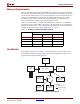
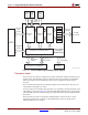
There are several interfaces to the integrated Endpoint block, including:
• Clock and Reset interface, as described in “Clock and Reset Interface,” page 21.
• Transaction Layer interface, as described in “Transaction Layer Interface,” page 28.
• Management interface, as described in “Management Interface,” page 37.
• Memory interface, as described in “Block RAM Interface,” page 40.
• Transceiver interface, as described in “Transceiver Interface,” page 42.
• Configuration and Status interface, as described in “Configuration and Status
Interface,” page 46.
The Transceiver interface, the Memory interface, and the Clock and Reset interface are
automatically connected in the CORE Generator wrappers. These interfaces are not visible
outside of the wrappers. The Transaction Layer interface must interface with the user
design in fabric. The rest of the interfaces are optional; the user can choose whether to
access them, and which pins to access.