
Instruction manual


PC27E Page 13
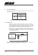
Channel Input Pin Attenuator Resistor Positions
Nº SK1 Input Ground
0 4 RN2 - A RN4 pin 2
1 5 RN2 - B RN4 pin 3
2 6 RN2 - C RN4 pin 4
3 7 RN2 - D RN4 pin 5
4 8 RN2 - E RN4 pin 6
5 9 RN2 - F RN4 pin 7
6 10 RN2 - G RN4 pin 8
7 11 RN2 - H RN4 pin 9
8 12 RN3 - A RN5 pin 9
9 13 RN3 - B RN5 pin 8
10 14 RN3 - C RN5 pin 7
11 15 RN3 - D RN5 pin 6
12 16 RN3 - E RN5 pin 5
13 17 RN3 - F RN5 pin 4
14 18 RN3 - G RN5 pin 3
15 19 RN3 - H RN5 pin 2
For example, to obtain a range of ±25 volts on analog input channel 0, while retaining ranging
of ±2 volts on the other 15 channels:
1. Insert a single in-line resistor network in position RN4. 100kΩ would be a
suitable value. (If only one channel is to be equipped with an attenuator, then a single
100kΩ resistor can be inserted between RN4 pins 1 and 2).
2. Drill out the drill point at RN2 - A using a 1mm drill, leaving the position clear
to insert a resistor.
3. Calculate the required input resistor, Rin, thus:-
The maximum input voltage to the multiplexer must be ±2 volts for a full scale
reading, with Vin ±25 volts maximum.
Full scale reading 100k
---------------------------------- = ---------------
Maximum input voltage 100k + Rin
( Maximum input voltage )
Rin = (100k x ----------------------------------- ) - 100k
( Full scale reading )
Rin = (100k x 25/2 ) - 100k = 1.15MΩ
4. Insert a 1.15MΩ high stability resistor in the position vacated by drilling out
RN2 - A.