
Instruction manual


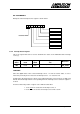


Table Of Contents
- INTRODUCTION
- GETTING STARTED
- MAKING THE CONNECTIONS
- USING THE PC215E
- STRUCTURE AND ASSIGNMENTS OF THE REGISTERS
- Register Assignments
- Register Groups
- The Register Details
- Programmable Peripheral Interface PPI-X Data Register Port A
- Programmable Peripheral Interface PPI-X Data Register Port B
- Programmable Peripheral Interface PPI-X Data Register Port C
- Programmable Peripheral Interface PPI-X Command Register
- Programmable Peripheral Interface PPI-Y Data Register Port A
- Programmable Peripheral Interface PPI-Y Data Register Port B
- Programmable Peripheral Interface PPI-Y Data Register Port C
- Programmable Peripheral Interface PPI-Y Command Register
- Z1 Counter 0 Data Register
- Z1 Counter 1 Data Register
- Z1 Counter 2 Data Register
- Counter/Timer Z1 Control Register
- Z1 Counter/Timer Status Register
- Z2 Counter 0 Data Register
- Z2 Counter 1 Data Register
- Z2 Counter 2 Data Register
- Counter/Timer Z2 Control Register
- Z2 Counter/Timer Status Register
- Group Z Clock Connection Register
- Group Z Gate Connection Register
- Interrupt Source Selection Register
- Interrupt Status Register
- PROGRAMMING THE PC215E
- Copyright
- Files installed from the Distribution Diskette
- Windows DLL and Examples
- DOS 'C' Library and Examples
- Using the Dynamic Link Library
- Windows and DOS Library Functions
- Initialisation Functions
- Interrupt Control Functions
- Data Buffer Functions
- Timer/Counter Functions
- Differential Counter Functions
- Frequency Generation Functions
- Millisecond Stopwatch Functions
- Frequency Input and Output Functions
- Digitally- and Voltage-Controlled Oscillator Functions
- Digital Input/Output Functions
- Switch Scanner Matrix Functions
- Bi-Directional Data Bus Functions
- PC215E Library Error Codes
- PC215E Interface Guide For LABTECH NOTEBOOK
- Guide to User Programming
- Signal Centre
- CONTENTS
- DECLARATION OF CONFORMITY
Page
49
PC215E
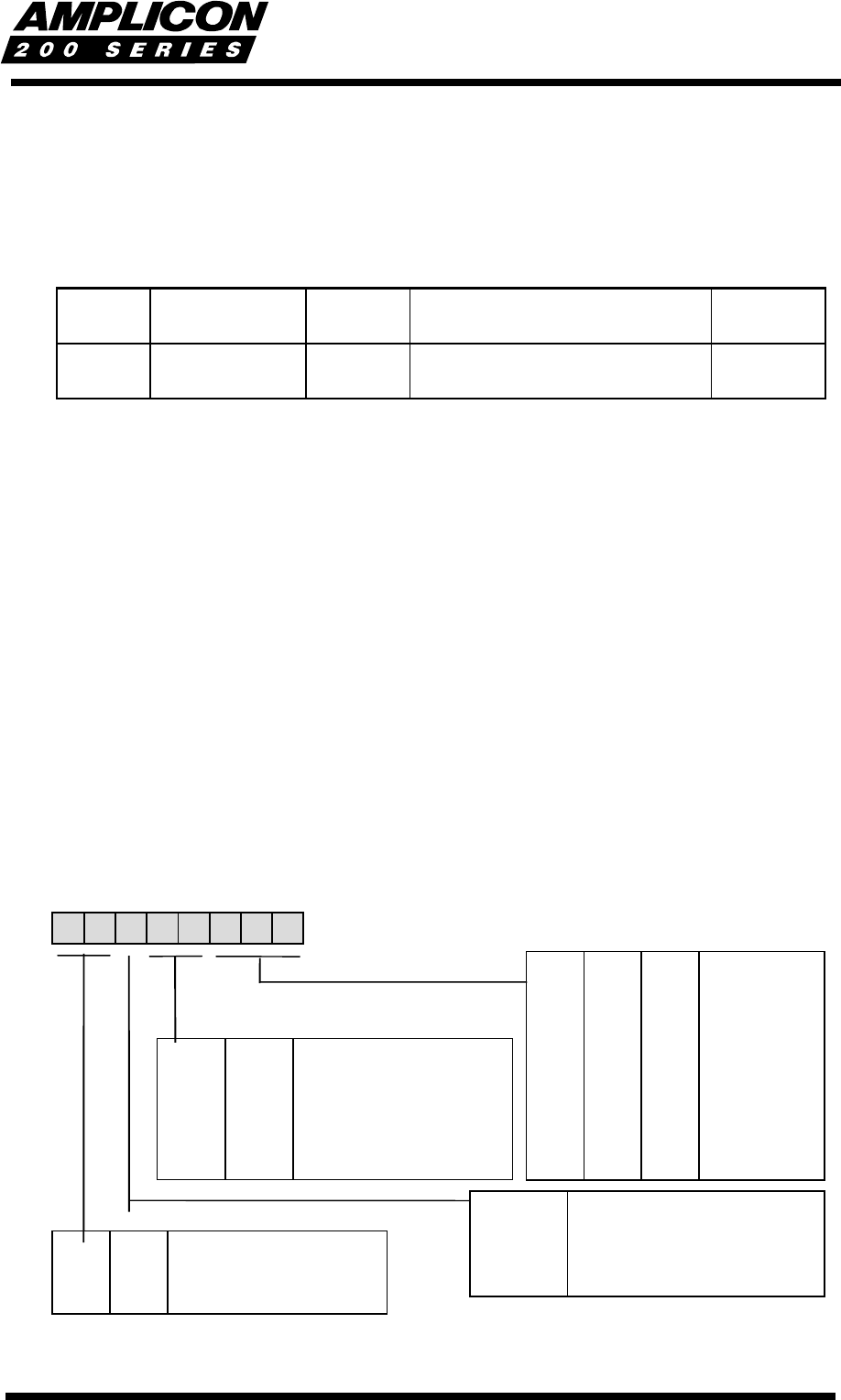
5.3.19 Group Z Clock Connection Register
This is the register that can be used to select the counter/timer clock sources for the six
counter/timers on the PC215E board.
Register
Offset
Write and/or
Read
Register
Width
Register
Title
Mnemonic
1A
16
Write 8 bits
Group Z Counter/timer Clock
Selection Register
ZCLK_SCE
FUNCTION
Individually selects one of the eight possible Counter/Timer clock sources for each of the six
counter/timers on the PC215E board. The selected source will then appear on the clock input of
the specified counter/timer.
The Eight Clock Sources
The eight possible clock sources are as follows:
1. The counter/timer's CLK input from the SK1 connector
2. The internal 10 MHz clock
3. The internal 1 MHz clock
4. The internal 100 kHz clock
5. The internal 10 kHz clock
6. The internal 1 kHz clock
7. The output of the preceding counter/timer
8. The dedicated external clock input for Z1/Z2
BIT ASSIGNMENTS
01234567
Clock Source
CLK n
10 MHz
1 MHz
100 kHz
10 kHz
1 kHz
OUT n-1
Ext Clock
bit 0
0
1
0
1
0
1
0
1
bit 1
0
0
1
1
0
0
1
1
bit 2
0
0
0
0
1
1
1
1
Counter/Timer
Counter 0
Counter 1
Counter 2
Reserved
bit 3
0
1
0
1
bit 4
0
0
1
1
Reserved
bit 6
X
bit 7
X
bit 5
0
1
Counter/Timer Device
Z1
Z2