
Instruction manual

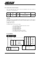


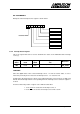


Table Of Contents
- INTRODUCTION
- GETTING STARTED
- MAKING THE CONNECTIONS
- USING THE PC215E
- STRUCTURE AND ASSIGNMENTS OF THE REGISTERS
- Register Assignments
- Register Groups
- The Register Details
- Programmable Peripheral Interface PPI-X Data Register Port A
- Programmable Peripheral Interface PPI-X Data Register Port B
- Programmable Peripheral Interface PPI-X Data Register Port C
- Programmable Peripheral Interface PPI-X Command Register
- Programmable Peripheral Interface PPI-Y Data Register Port A
- Programmable Peripheral Interface PPI-Y Data Register Port B
- Programmable Peripheral Interface PPI-Y Data Register Port C
- Programmable Peripheral Interface PPI-Y Command Register
- Z1 Counter 0 Data Register
- Z1 Counter 1 Data Register
- Z1 Counter 2 Data Register
- Counter/Timer Z1 Control Register
- Z1 Counter/Timer Status Register
- Z2 Counter 0 Data Register
- Z2 Counter 1 Data Register
- Z2 Counter 2 Data Register
- Counter/Timer Z2 Control Register
- Z2 Counter/Timer Status Register
- Group Z Clock Connection Register
- Group Z Gate Connection Register
- Interrupt Source Selection Register
- Interrupt Status Register
- PROGRAMMING THE PC215E
- Copyright
- Files installed from the Distribution Diskette
- Windows DLL and Examples
- DOS 'C' Library and Examples
- Using the Dynamic Link Library
- Windows and DOS Library Functions
- Initialisation Functions
- Interrupt Control Functions
- Data Buffer Functions
- Timer/Counter Functions
- Differential Counter Functions
- Frequency Generation Functions
- Millisecond Stopwatch Functions
- Frequency Input and Output Functions
- Digitally- and Voltage-Controlled Oscillator Functions
- Digital Input/Output Functions
- Switch Scanner Matrix Functions
- Bi-Directional Data Bus Functions
- PC215E Library Error Codes
- PC215E Interface Guide For LABTECH NOTEBOOK
- Guide to User Programming
- Signal Centre
- CONTENTS
- DECLARATION OF CONFORMITY
PC215E Page 48
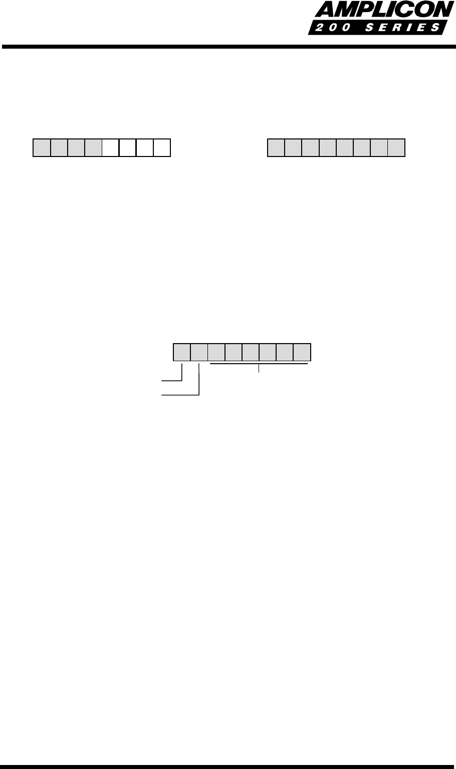
BIT ASSIGNMENTS
Bit layout of the counter/timer status word register is shown below.
Bits 5…0 Counter's programmed Mode exactly as written in the last Mode Control Word
Bit 6 State of the addressed counter element
0 Count available for reading
1 Null Count
Bit 7 State of the addressed counter OUT pin
0 OUT pin is '0'
1 OUT pin is '1'
01234567
Counter Latch Command
Bits 3 to 0 = Don’t care
Bits 5 and 4 = 0
Designates Counter Latch Command
Bits 7 and 6
00 = Counter 0
01 = Counter 1
10 = Counter 2
11 = Read-back Command
01234567
Read-back Command
Bit 0 = 0
Bit 1 = Select Counter 0
Bit 2 = Select Counter 1
Bit 3 = Select Counter 2
Bit 4 = /Latch Status of Selected Counter(s)
Bit 5 = /Latch Count of Selected Counter(s)
Bits 6 and 7 = 1
Designates Read-back Command
01234567
Counter Programmed
Mode
OUT Pin Status
Null Count