
Instruction manual


Table Of Contents
- INTRODUCTION
- GETTING STARTED
- MAKING THE CONNECTIONS
- USING THE PC215E
- STRUCTURE AND ASSIGNMENTS OF THE REGISTERS
- Register Assignments
- Register Groups
- The Register Details
- Programmable Peripheral Interface PPI-X Data Register Port A
- Programmable Peripheral Interface PPI-X Data Register Port B
- Programmable Peripheral Interface PPI-X Data Register Port C
- Programmable Peripheral Interface PPI-X Command Register
- Programmable Peripheral Interface PPI-Y Data Register Port A
- Programmable Peripheral Interface PPI-Y Data Register Port B
- Programmable Peripheral Interface PPI-Y Data Register Port C
- Programmable Peripheral Interface PPI-Y Command Register
- Z1 Counter 0 Data Register
- Z1 Counter 1 Data Register
- Z1 Counter 2 Data Register
- Counter/Timer Z1 Control Register
- Z1 Counter/Timer Status Register
- Z2 Counter 0 Data Register
- Z2 Counter 1 Data Register
- Z2 Counter 2 Data Register
- Counter/Timer Z2 Control Register
- Z2 Counter/Timer Status Register
- Group Z Clock Connection Register
- Group Z Gate Connection Register
- Interrupt Source Selection Register
- Interrupt Status Register
- PROGRAMMING THE PC215E
- Copyright
- Files installed from the Distribution Diskette
- Windows DLL and Examples
- DOS 'C' Library and Examples
- Using the Dynamic Link Library
- Windows and DOS Library Functions
- Initialisation Functions
- Interrupt Control Functions
- Data Buffer Functions
- Timer/Counter Functions
- Differential Counter Functions
- Frequency Generation Functions
- Millisecond Stopwatch Functions
- Frequency Input and Output Functions
- Digitally- and Voltage-Controlled Oscillator Functions
- Digital Input/Output Functions
- Switch Scanner Matrix Functions
- Bi-Directional Data Bus Functions
- PC215E Library Error Codes
- PC215E Interface Guide For LABTECH NOTEBOOK
- Guide to User Programming
- Signal Centre
- CONTENTS
- DECLARATION OF CONFORMITY
Page
45
PC215E
FUNCTION
The Z2 Counter 2 Data Register is used to write and read 8 bit data to the 82C54 Z2
counter/timer 2. The counter is normally configured for 16 bit operation and to ensure validity of
the data. It is important to always write/read two bytes to the register, least significant byte first.
Please note that the 16-bit count values written to this register are not latched into the counting
element until the next clock pulse (assuming the gate input is high). Subsequent read
operations from this register will therefore not reflect the new count value until this clock pulse
has latched the data.
The input to counter 2 can be any of the five internal master clock frequencies (10MHz, 1 MHz,
100 KHz, 10 kHz or 1 kHz), an external clock, the Z2 External Clock signal or the output of Z2
counter 1. This clock source selection is made by writing to the Group Z Clock Connection
Register described in Section 5.3.19.
The output of counter 2 is available on the user socket, SK1 pin 20, and also as a possible clock
source for Z1 counter 0.
The gate input to counter 2 can be selected as VCC (permanently enabled), GND (permanently
disabled), the inverted output of Z2 Counter 0, or an external gate signal on SK1 pin 78. This
gate selection is made by writing to the Group Z Gate Connection Register described in Section
5.3.20.
Further information on programming the 82C54 Programmable Counter/Timer is given in
chapters 4 and 6.
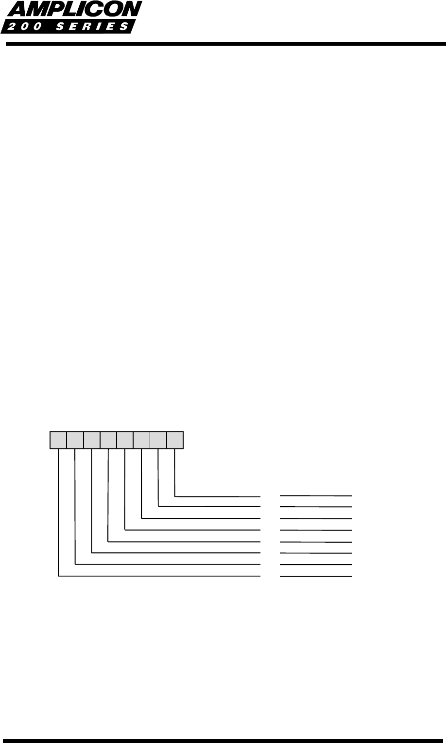
BIT ASSIGNMENTS
The bit layout of the Z2 counter 2 data register is shown below.
5.3.17 Counter/Timer Z2 Control Register
The Z2 control register provides the means to configure the three sixteen bit counter/timers of
the 82C54 Z2. An outline of its operation is given here, but reference should be made to the
82C54 device manufacturers’ data sheets in the appendices before programming of the counter
is attempted.
The Counter Timer Control register is a WRITE register. The READ register at the same
location BA + 13
16
returns the status of the 82C54 Z2 Counter/Timer when used with the Read-
Back command.
01234567
Second Byte
(Most Significant)
8
9
10
11
12
13
14
15
First Byte
(Least Significant)
0
1
2
3
4
5
6
7
Z2 16 BIT COUNTER 2 DATA BIT