
Instruction manual


Table Of Contents
- INTRODUCTION
- GETTING STARTED
- MAKING THE CONNECTIONS
- USING THE PC215E
- STRUCTURE AND ASSIGNMENTS OF THE REGISTERS
- Register Assignments
- Register Groups
- The Register Details
- Programmable Peripheral Interface PPI-X Data Register Port A
- Programmable Peripheral Interface PPI-X Data Register Port B
- Programmable Peripheral Interface PPI-X Data Register Port C
- Programmable Peripheral Interface PPI-X Command Register
- Programmable Peripheral Interface PPI-Y Data Register Port A
- Programmable Peripheral Interface PPI-Y Data Register Port B
- Programmable Peripheral Interface PPI-Y Data Register Port C
- Programmable Peripheral Interface PPI-Y Command Register
- Z1 Counter 0 Data Register
- Z1 Counter 1 Data Register
- Z1 Counter 2 Data Register
- Counter/Timer Z1 Control Register
- Z1 Counter/Timer Status Register
- Z2 Counter 0 Data Register
- Z2 Counter 1 Data Register
- Z2 Counter 2 Data Register
- Counter/Timer Z2 Control Register
- Z2 Counter/Timer Status Register
- Group Z Clock Connection Register
- Group Z Gate Connection Register
- Interrupt Source Selection Register
- Interrupt Status Register
- PROGRAMMING THE PC215E
- Copyright
- Files installed from the Distribution Diskette
- Windows DLL and Examples
- DOS 'C' Library and Examples
- Using the Dynamic Link Library
- Windows and DOS Library Functions
- Initialisation Functions
- Interrupt Control Functions
- Data Buffer Functions
- Timer/Counter Functions
- Differential Counter Functions
- Frequency Generation Functions
- Millisecond Stopwatch Functions
- Frequency Input and Output Functions
- Digitally- and Voltage-Controlled Oscillator Functions
- Digital Input/Output Functions
- Switch Scanner Matrix Functions
- Bi-Directional Data Bus Functions
- PC215E Library Error Codes
- PC215E Interface Guide For LABTECH NOTEBOOK
- Guide to User Programming
- Signal Centre
- CONTENTS
- DECLARATION OF CONFORMITY
PC215E Page 44
The output of counter 1 is available on the user socket, SK1 pin 58, and also as a possible clock
source for counter 2.
The gate input to counter 1 can be selected as VCC (permanently enabled), GND (permanently
disabled), the inverted output of Z1 Counter 2, or an external gate signal on SK1 pin 19. This
gate selection is made by writing to the Group Z Gate Connection Register described in Section
5.3.20.
Further information on programming the 82C54 Programmable Counter/Timer is given in
chapters 4 and 6.
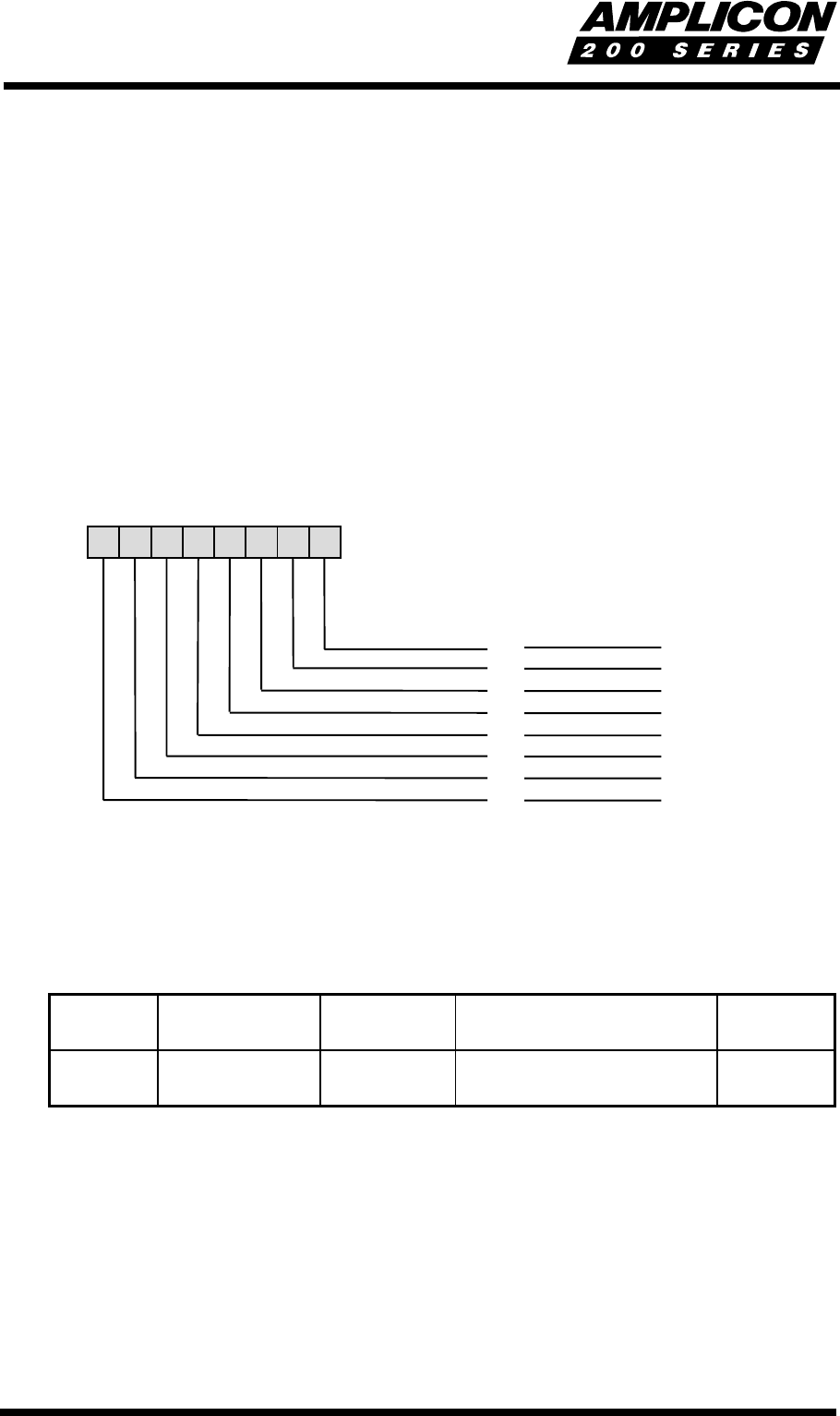
BIT ASSIGNMENTS
The bit layout of the Z2 counter 1 data register is shown below.
5.3.16 Z2 Counter 2 Data Register
The 82C54 Programmable Timer Counter Z2 provides three 16 bit counter/timers which can be
independently programmed to operate in any one of six modes with BCD or Binary count
functions. The register definition for Z2 Counter 2 Data is as follows.
Register
Offset
Write and/or
Read
Register
Width
Register
Title
Mnemonic
16
16
Write and Read 8 bits
82C54 Z2 Counter/Timer
Counter 2 Data Register
Z2 CT2
01234567
Second Byte
(Most Significant)
8
9
10
11
12
13
14
15
First Byte
(Least Significant)
0
1
2
3
4
5
6
7
Z2 16 BIT COUNTER 1 DATA BIT