
Instruction manual
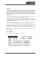


Table Of Contents
- INTRODUCTION
- GETTING STARTED
- MAKING THE CONNECTIONS
- USING THE PC215E
- STRUCTURE AND ASSIGNMENTS OF THE REGISTERS
- Register Assignments
- Register Groups
- The Register Details
- Programmable Peripheral Interface PPI-X Data Register Port A
- Programmable Peripheral Interface PPI-X Data Register Port B
- Programmable Peripheral Interface PPI-X Data Register Port C
- Programmable Peripheral Interface PPI-X Command Register
- Programmable Peripheral Interface PPI-Y Data Register Port A
- Programmable Peripheral Interface PPI-Y Data Register Port B
- Programmable Peripheral Interface PPI-Y Data Register Port C
- Programmable Peripheral Interface PPI-Y Command Register
- Z1 Counter 0 Data Register
- Z1 Counter 1 Data Register
- Z1 Counter 2 Data Register
- Counter/Timer Z1 Control Register
- Z1 Counter/Timer Status Register
- Z2 Counter 0 Data Register
- Z2 Counter 1 Data Register
- Z2 Counter 2 Data Register
- Counter/Timer Z2 Control Register
- Z2 Counter/Timer Status Register
- Group Z Clock Connection Register
- Group Z Gate Connection Register
- Interrupt Source Selection Register
- Interrupt Status Register
- PROGRAMMING THE PC215E
- Copyright
- Files installed from the Distribution Diskette
- Windows DLL and Examples
- DOS 'C' Library and Examples
- Using the Dynamic Link Library
- Windows and DOS Library Functions
- Initialisation Functions
- Interrupt Control Functions
- Data Buffer Functions
- Timer/Counter Functions
- Differential Counter Functions
- Frequency Generation Functions
- Millisecond Stopwatch Functions
- Frequency Input and Output Functions
- Digitally- and Voltage-Controlled Oscillator Functions
- Digital Input/Output Functions
- Switch Scanner Matrix Functions
- Bi-Directional Data Bus Functions
- PC215E Library Error Codes
- PC215E Interface Guide For LABTECH NOTEBOOK
- Guide to User Programming
- Signal Centre
- CONTENTS
- DECLARATION OF CONFORMITY

Page
41
PC215E
5.3.13 Z1 Counter/Timer Status Register
This status register provides the means to interrogate the three sixteen bit counter/timers of the
82C54 Z1. An outline of its operation is given here, but reference should be made to the 82C54
device manufacturers’ data sheets in the appendix before programming of the counter is
attempted.
The Z1 counter Status Register is a READ register. The WRITE register at the same location
BA + 13
16
controls the operation of the 82C54 Counter/Timer Z1 and issues a Read-Back
command before the status is interrogated.
Register
Offset
Write and/or
Read
Register
Width
Register
Title
Mnemonic
13
16
Read 8 bits
82C54 Z1 Counter/Timer
Status Register
Z1 CTS
FUNCTION
When the Read-Back Command requests the status of the counters, the status register provides
the count value, programmed mode, the current state of the OUT pin and Null Count Flag of the
selected counter(s).
BIT ASSIGNMENTS
Bit layout of the counter/timer status word register is shown below.
01234567
Counter Latch Command
Bits 3 to 0 = Don’t care
Bits 5 and 4 = 0
Designates Counter Latch Command
Bits 7 and 6
00 = Counter 0
01 = Counter 1
10 = Counter 2
11 = Read-back Command
01234567
Read-back Command
Bit 0 = 0
Bit 1 = Select Counter 0
Bit 2 = Select Counter 1
Bit 3 = Select Counter 2
Bit 4 = /Latch Status of Selected Counter(s)
Bit 5 = /Latch Count of Selected Counter(s)
Bits 6 and 7 = 1
Designates Read-back Command
01234567
Counter Programmed
Mode
OUT Pin Status
Null Count