
Instruction manual


Table Of Contents
- INTRODUCTION
- GETTING STARTED
- MAKING THE CONNECTIONS
- USING THE PC215E
- STRUCTURE AND ASSIGNMENTS OF THE REGISTERS
- Register Assignments
- Register Groups
- The Register Details
- Programmable Peripheral Interface PPI-X Data Register Port A
- Programmable Peripheral Interface PPI-X Data Register Port B
- Programmable Peripheral Interface PPI-X Data Register Port C
- Programmable Peripheral Interface PPI-X Command Register
- Programmable Peripheral Interface PPI-Y Data Register Port A
- Programmable Peripheral Interface PPI-Y Data Register Port B
- Programmable Peripheral Interface PPI-Y Data Register Port C
- Programmable Peripheral Interface PPI-Y Command Register
- Z1 Counter 0 Data Register
- Z1 Counter 1 Data Register
- Z1 Counter 2 Data Register
- Counter/Timer Z1 Control Register
- Z1 Counter/Timer Status Register
- Z2 Counter 0 Data Register
- Z2 Counter 1 Data Register
- Z2 Counter 2 Data Register
- Counter/Timer Z2 Control Register
- Z2 Counter/Timer Status Register
- Group Z Clock Connection Register
- Group Z Gate Connection Register
- Interrupt Source Selection Register
- Interrupt Status Register
- PROGRAMMING THE PC215E
- Copyright
- Files installed from the Distribution Diskette
- Windows DLL and Examples
- DOS 'C' Library and Examples
- Using the Dynamic Link Library
- Windows and DOS Library Functions
- Initialisation Functions
- Interrupt Control Functions
- Data Buffer Functions
- Timer/Counter Functions
- Differential Counter Functions
- Frequency Generation Functions
- Millisecond Stopwatch Functions
- Frequency Input and Output Functions
- Digitally- and Voltage-Controlled Oscillator Functions
- Digital Input/Output Functions
- Switch Scanner Matrix Functions
- Bi-Directional Data Bus Functions
- PC215E Library Error Codes
- PC215E Interface Guide For LABTECH NOTEBOOK
- Guide to User Programming
- Signal Centre
- CONTENTS
- DECLARATION OF CONFORMITY
Page
39
PC215E
Further information on programming the 82C54 Programmable Counter/Timer is given in
chapters 4 and 6.
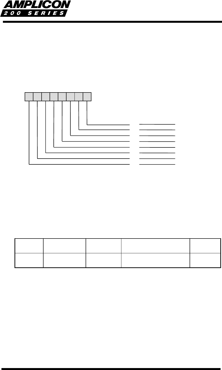
BIT ASSIGNMENTS
The bit layout of the Z1 counter 2 data register is shown below.
5.3.12 Counter/Timer Z1 Control Register
The Z1 control register provides the means to configure the three sixteen bit counter/timers of
the 82C54 Z1. An outline of its operation is given here, but reference should be made to the
82C54 device manufacturers’ data sheets in the appendices before programming of the counter
is attempted.
The Counter Timer Control register is a WRITE register. The READ register at the same
location BA + 13
16
returns the status of the 82C54 Z1 Counter/Timer when used with the Read-
Back command.
Register
Offset
Write and/or
Read
Register
Width
Register
Title
Mnemonic
13
16
Write 8 bits
82C54 Z1 Counter/Timer
Control Register
Z1 CTC
FUNCTION
Provides a control word to define the operation of the Z1 counters 0, 1 and 2.
The programming procedure for the 82C54 is flexible, but the following two conventions must be
followed:
• For each counter, the control word must be written before the initial count is loaded.
• The initial count must follow the count format specified in the control word. This format is
normally least significant byte followed by most significant byte (control word bits 5, 4 = 1 1)
but can be L.S. byte only or M.S. byte only.
01234567
Second Byte
(Most Significant)
8
9
10
11
12
13
14
15
First Byte
(Least Significant)
0
1
2
3
4
5
6
7
Z1 16 BIT COUNTER 2 DATA BIT