
Instruction manual
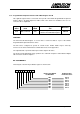
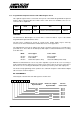


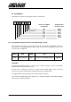

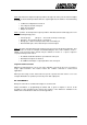
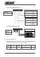
Table Of Contents
- INTRODUCTION
- GETTING STARTED
- MAKING THE CONNECTIONS
- USING THE PC215E
- STRUCTURE AND ASSIGNMENTS OF THE REGISTERS
- Register Assignments
- Register Groups
- The Register Details
- Programmable Peripheral Interface PPI-X Data Register Port A
- Programmable Peripheral Interface PPI-X Data Register Port B
- Programmable Peripheral Interface PPI-X Data Register Port C
- Programmable Peripheral Interface PPI-X Command Register
- Programmable Peripheral Interface PPI-Y Data Register Port A
- Programmable Peripheral Interface PPI-Y Data Register Port B
- Programmable Peripheral Interface PPI-Y Data Register Port C
- Programmable Peripheral Interface PPI-Y Command Register
- Z1 Counter 0 Data Register
- Z1 Counter 1 Data Register
- Z1 Counter 2 Data Register
- Counter/Timer Z1 Control Register
- Z1 Counter/Timer Status Register
- Z2 Counter 0 Data Register
- Z2 Counter 1 Data Register
- Z2 Counter 2 Data Register
- Counter/Timer Z2 Control Register
- Z2 Counter/Timer Status Register
- Group Z Clock Connection Register
- Group Z Gate Connection Register
- Interrupt Source Selection Register
- Interrupt Status Register
- PROGRAMMING THE PC215E
- Copyright
- Files installed from the Distribution Diskette
- Windows DLL and Examples
- DOS 'C' Library and Examples
- Using the Dynamic Link Library
- Windows and DOS Library Functions
- Initialisation Functions
- Interrupt Control Functions
- Data Buffer Functions
- Timer/Counter Functions
- Differential Counter Functions
- Frequency Generation Functions
- Millisecond Stopwatch Functions
- Frequency Input and Output Functions
- Digitally- and Voltage-Controlled Oscillator Functions
- Digital Input/Output Functions
- Switch Scanner Matrix Functions
- Bi-Directional Data Bus Functions
- PC215E Library Error Codes
- PC215E Interface Guide For LABTECH NOTEBOOK
- Guide to User Programming
- Signal Centre
- CONTENTS
- DECLARATION OF CONFORMITY
Page
35
PC215E
Command Word for Mode Definition Format
Command Word for Bit Set/Reset Format
5.3.9 Z1 Counter 0 Data Register
The 82C54 Programmable Timer Counter Z1 provides three 16 bit counter/timers which can be
independently programmed to operate in any one of six modes with BCD or Binary count
functions. The register definition for Z1 Counter 0 Data is as follows.
Register
Offset
Write and/or
Read
Register
Width
Register
Title
Mnemonic
10
16
Write and Read 8 bits
82C54 Counter/Timer Z1
Counter 0 Data Register
Z1 CT0
01234567
Port C (Lower) 0 = Output
1 = Input
Port B 0 = Output
1 = Input
Mode Selection 0 = Mode 0
1 = Mode 1
GROUP B
Port C (Upper) 0 = Output
1 = Input
Port A 0 = Output
1 = Input
Mode Selection 00 = Mode 0
01 = Mode 1
1X = Mode 2
GROUP A
e
Set Flag 1 = Active
COMMAND
SELECT
01234567
Bit Set/Reset 0 = Reset
1 = Set
Port C Bit Select
Bit Set/Reset Flag
0 = Active
COMMAND
SELECT
6 74 5
2 3
0 1
0 B
0
10 1
0 1
0 1
1 B
1
10 01 10 0
1 B
2
11 10 00 0
X X X
Don't Care