
Instruction manual


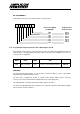

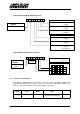
Table Of Contents
- INTRODUCTION
- GETTING STARTED
- MAKING THE CONNECTIONS
- USING THE PC215E
- STRUCTURE AND ASSIGNMENTS OF THE REGISTERS
- Register Assignments
- Register Groups
- The Register Details
- Programmable Peripheral Interface PPI-X Data Register Port A
- Programmable Peripheral Interface PPI-X Data Register Port B
- Programmable Peripheral Interface PPI-X Data Register Port C
- Programmable Peripheral Interface PPI-X Command Register
- Programmable Peripheral Interface PPI-Y Data Register Port A
- Programmable Peripheral Interface PPI-Y Data Register Port B
- Programmable Peripheral Interface PPI-Y Data Register Port C
- Programmable Peripheral Interface PPI-Y Command Register
- Z1 Counter 0 Data Register
- Z1 Counter 1 Data Register
- Z1 Counter 2 Data Register
- Counter/Timer Z1 Control Register
- Z1 Counter/Timer Status Register
- Z2 Counter 0 Data Register
- Z2 Counter 1 Data Register
- Z2 Counter 2 Data Register
- Counter/Timer Z2 Control Register
- Z2 Counter/Timer Status Register
- Group Z Clock Connection Register
- Group Z Gate Connection Register
- Interrupt Source Selection Register
- Interrupt Status Register
- PROGRAMMING THE PC215E
- Copyright
- Files installed from the Distribution Diskette
- Windows DLL and Examples
- DOS 'C' Library and Examples
- Using the Dynamic Link Library
- Windows and DOS Library Functions
- Initialisation Functions
- Interrupt Control Functions
- Data Buffer Functions
- Timer/Counter Functions
- Differential Counter Functions
- Frequency Generation Functions
- Millisecond Stopwatch Functions
- Frequency Input and Output Functions
- Digitally- and Voltage-Controlled Oscillator Functions
- Digital Input/Output Functions
- Switch Scanner Matrix Functions
- Bi-Directional Data Bus Functions
- PC215E Library Error Codes
- PC215E Interface Guide For LABTECH NOTEBOOK
- Guide to User Programming
- Signal Centre
- CONTENTS
- DECLARATION OF CONFORMITY

PC215E Page 34
Mode 0 provides basic input and output operations through each of the ports A, B and C. Output
data bits are latched and input data follows the signals applied to the I/O lines. No handshaking
is needed.
• 16 different configurations in mode 0
• Two 8 bit ports and two 4 bit ports
• Inputs are not latched
• Outputs are latched
Mode 1 provides strobed input and output operations with data transferred through port A or B
and handshaking through port C.
• Two I/O groups (Group A - also known as Group 0 or Group I)
• (Group B - also known as Group 1 or Group II)
• Both groups contain an 8 bit port and a 4 bit control/data port
• Both 8 bit data ports can be latched input or latched output
Mode 2 provides strobed bi-directional operation using port A as the bi-directional data bus. Port
C3 to C7 bits are used for interrupts and handshaking bus flow control similar to mode 1.
NOTE: Port B and port C0 to C2 bits may be defined as mode 0 or 1, input or output in
conjunction with port A in mode 2.
• An 8 bit latched bi-directional bus port and 5 bit control port
• Both input and outputs are latched
• An additional 8 bit input or output port with a 3 bit control port
Single Bit Set/Reset Feature
With bit 7 'Command Select' set to '0', any of the eight bits of port C can be set or reset using a
single output instruction. This feature reduces the software overhead in control based
applications.
When port C is being used as status/control for port A or port B, these bits can be set or reset
using the Bit Set/Reset operation just as if they were data output ports.
BIT ASSIGNMENTS
Bit layouts of the PPI-Y command word register is shown below.
Further information on programming the 82C55 PPI is given in chapters 4 and 6. A full
description of the operating modes and all other features of the 82C55 are available in the
82C55 device manufacturer's data sheet in the appendices.