
Instruction manual
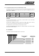


Table Of Contents
- INTRODUCTION
- GETTING STARTED
- MAKING THE CONNECTIONS
- USING THE PC215E
- STRUCTURE AND ASSIGNMENTS OF THE REGISTERS
- Register Assignments
- Register Groups
- The Register Details
- Programmable Peripheral Interface PPI-X Data Register Port A
- Programmable Peripheral Interface PPI-X Data Register Port B
- Programmable Peripheral Interface PPI-X Data Register Port C
- Programmable Peripheral Interface PPI-X Command Register
- Programmable Peripheral Interface PPI-Y Data Register Port A
- Programmable Peripheral Interface PPI-Y Data Register Port B
- Programmable Peripheral Interface PPI-Y Data Register Port C
- Programmable Peripheral Interface PPI-Y Command Register
- Z1 Counter 0 Data Register
- Z1 Counter 1 Data Register
- Z1 Counter 2 Data Register
- Counter/Timer Z1 Control Register
- Z1 Counter/Timer Status Register
- Z2 Counter 0 Data Register
- Z2 Counter 1 Data Register
- Z2 Counter 2 Data Register
- Counter/Timer Z2 Control Register
- Z2 Counter/Timer Status Register
- Group Z Clock Connection Register
- Group Z Gate Connection Register
- Interrupt Source Selection Register
- Interrupt Status Register
- PROGRAMMING THE PC215E
- Copyright
- Files installed from the Distribution Diskette
- Windows DLL and Examples
- DOS 'C' Library and Examples
- Using the Dynamic Link Library
- Windows and DOS Library Functions
- Initialisation Functions
- Interrupt Control Functions
- Data Buffer Functions
- Timer/Counter Functions
- Differential Counter Functions
- Frequency Generation Functions
- Millisecond Stopwatch Functions
- Frequency Input and Output Functions
- Digitally- and Voltage-Controlled Oscillator Functions
- Digital Input/Output Functions
- Switch Scanner Matrix Functions
- Bi-Directional Data Bus Functions
- PC215E Library Error Codes
- PC215E Interface Guide For LABTECH NOTEBOOK
- Guide to User Programming
- Signal Centre
- CONTENTS
- DECLARATION OF CONFORMITY
Page
29
PC215E
Mode 2 provides strobed bi-directional operation using port A as the bi-directional data bus. Port
C3 to C7 bits are used for interrupts and handshaking bus flow control similar to mode 1.
NOTE: Port B and port C0 to C2 bits may be defined as mode 0 or 1, input or output in
conjunction with port A in mode 2.
• An 8 bit latched bi-directional bus port and 5 bit control port
• Both input and outputs are latched
• An additional 8 bit input or output port with a 3 bit control port
Single Bit Set/Reset Feature
With bit 7 'Command Select' set to '0', any of the eight bits of port C can be set or reset using a
single output instruction. This feature reduces the software overhead in control based
applications.
When port C is being used as status/control for port A or port B, these bits can be set or reset
using the Bit Set/Reset operation just as if they were data output ports.
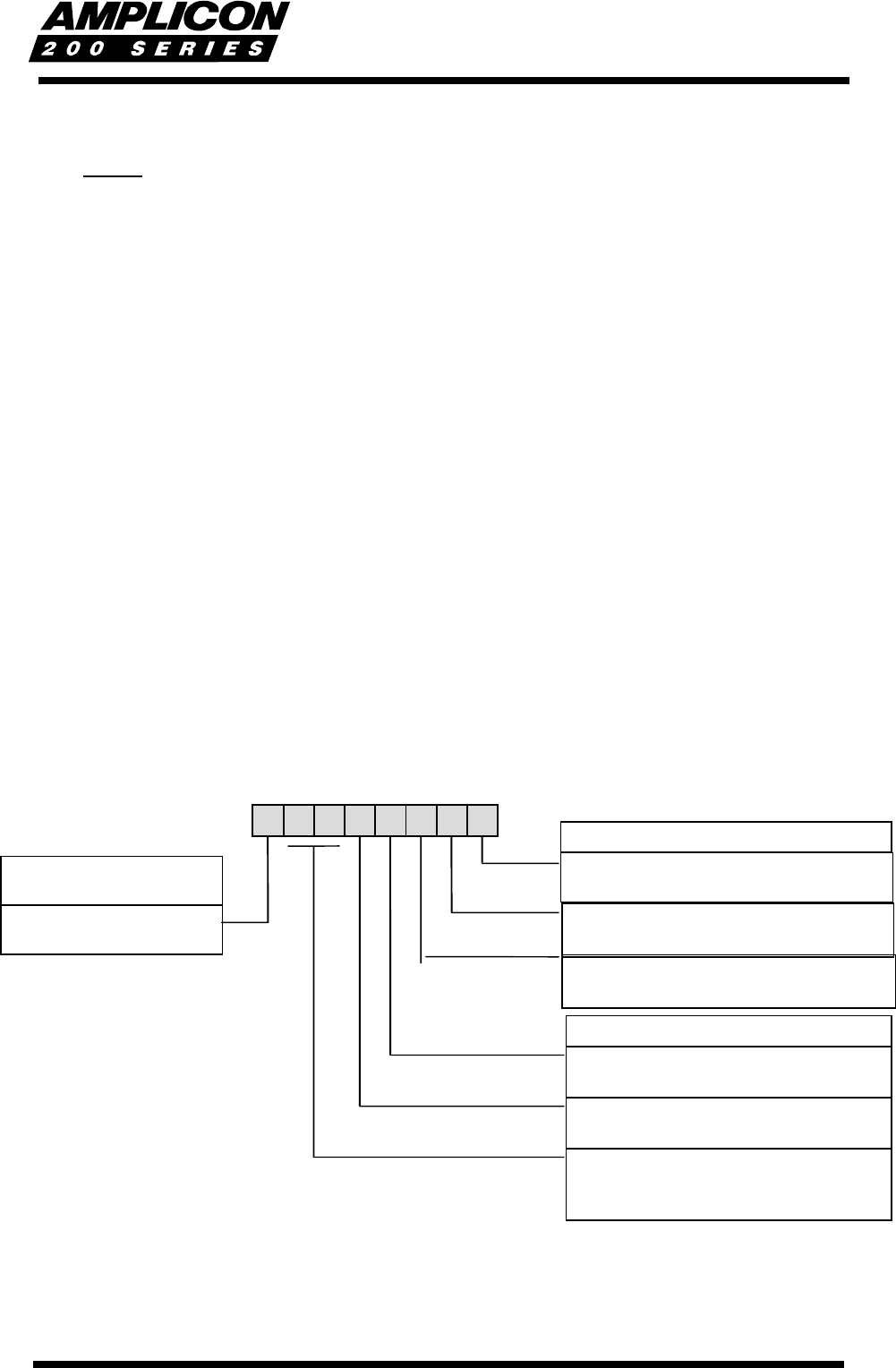
BIT ASSIGNMENTS
Bit layouts of the PPI-X command word register is shown below.
Further information on programming the 82C55 PPI is given in chapters 4 and 6. A full
description of the operating modes and all other features of the 82C55 are available in the
82C55 device manufacturer's data sheet in the appendices.
Command Word for Mode Definition Format
01234567
Port C (Lower) 0 = Output
1 = Input
Port B 0 = Output
1 = Input
Mode Selection 0 = Mode 0
1 = Mode 1
GROUP B
Port C (Upper) 0 = Output
1 = Input
Port A 0 = Output
1 = Input
Mode Selection 00 = Mode 0
01 = Mode 1
1X = Mode 2
GROUP A
e
Set Flag 1 = Active
COMMAND
SELECT