
Instruction manual


Table Of Contents
- INTRODUCTION
- GETTING STARTED
- MAKING THE CONNECTIONS
- USING THE PC215E
- STRUCTURE AND ASSIGNMENTS OF THE REGISTERS
- Register Assignments
- Register Groups
- The Register Details
- Programmable Peripheral Interface PPI-X Data Register Port A
- Programmable Peripheral Interface PPI-X Data Register Port B
- Programmable Peripheral Interface PPI-X Data Register Port C
- Programmable Peripheral Interface PPI-X Command Register
- Programmable Peripheral Interface PPI-Y Data Register Port A
- Programmable Peripheral Interface PPI-Y Data Register Port B
- Programmable Peripheral Interface PPI-Y Data Register Port C
- Programmable Peripheral Interface PPI-Y Command Register
- Z1 Counter 0 Data Register
- Z1 Counter 1 Data Register
- Z1 Counter 2 Data Register
- Counter/Timer Z1 Control Register
- Z1 Counter/Timer Status Register
- Z2 Counter 0 Data Register
- Z2 Counter 1 Data Register
- Z2 Counter 2 Data Register
- Counter/Timer Z2 Control Register
- Z2 Counter/Timer Status Register
- Group Z Clock Connection Register
- Group Z Gate Connection Register
- Interrupt Source Selection Register
- Interrupt Status Register
- PROGRAMMING THE PC215E
- Copyright
- Files installed from the Distribution Diskette
- Windows DLL and Examples
- DOS 'C' Library and Examples
- Using the Dynamic Link Library
- Windows and DOS Library Functions
- Initialisation Functions
- Interrupt Control Functions
- Data Buffer Functions
- Timer/Counter Functions
- Differential Counter Functions
- Frequency Generation Functions
- Millisecond Stopwatch Functions
- Frequency Input and Output Functions
- Digitally- and Voltage-Controlled Oscillator Functions
- Digital Input/Output Functions
- Switch Scanner Matrix Functions
- Bi-Directional Data Bus Functions
- PC215E Library Error Codes
- PC215E Interface Guide For LABTECH NOTEBOOK
- Guide to User Programming
- Signal Centre
- CONTENTS
- DECLARATION OF CONFORMITY
Page
21
PC215E
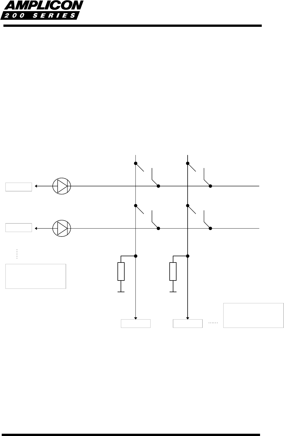
4.2.11 Switch Matrix
The high number of digital I/O channels available on the PC215E board lends itself to a switch
matrix scanner implementation. The status of a matrix of switches can be obtained by sending
test patterns into the matrix, and then reading status patterns back from the matrix.
Section 6.6.11 describes functions which allows either PPIX, or both PPIX and PPIY to be used
as such a device. Using only PPIX up to 144 switches can be scanned, and using both PPIX
and PPIY up to 576 switches can be scanned. Group A ports of the 82C55 device(s) - Port A
and Port C-upper - are set for output to send test patterns to the matrix, and group B ports - Port
B and Port C-lower - are set for input to read the switch status information. The user must
ensure that the switch matrix is wired as detailed below.
GND GND
1N4448
1N4448
SPST SPST
10k
Ω
10k
Ω
SPST SPST
PPI X A0
PPI X A1
PPI X B0 PPI X B1
etc., up to PPI X A7,
then C4 to C7, then
onto PPI Y, and PPI Z.
etc., up to PPI X B7,
then C0 to C3, then
onto PPI Y, and PPI Z.
Figure 7 - Switch Matrix Configuration
Function
DIOsetSwitchMatrix
allows you to setup the matrix, specifying the matrix order. For
the PC215E, this can be 12 X 12 or 24 X 24 switches. The function also registers the PPIs used
as being 'in use' and unavailable for use by other programs. Function DIOgetSwitchStatus
returns the status of a given switch in the matrix, and function
DIOfreeSwitchMatrix
frees the
PPIs so they can be used by other programs when the switch matrix is no longer required.