
Instruction manual
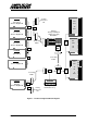
Table Of Contents
- INTRODUCTION
- GETTING STARTED
- MAKING THE CONNECTIONS
- USING THE PC215E
- STRUCTURE AND ASSIGNMENTS OF THE REGISTERS
- Register Assignments
- Register Groups
- The Register Details
- Programmable Peripheral Interface PPI-X Data Register Port A
- Programmable Peripheral Interface PPI-X Data Register Port B
- Programmable Peripheral Interface PPI-X Data Register Port C
- Programmable Peripheral Interface PPI-X Command Register
- Programmable Peripheral Interface PPI-Y Data Register Port A
- Programmable Peripheral Interface PPI-Y Data Register Port B
- Programmable Peripheral Interface PPI-Y Data Register Port C
- Programmable Peripheral Interface PPI-Y Command Register
- Z1 Counter 0 Data Register
- Z1 Counter 1 Data Register
- Z1 Counter 2 Data Register
- Counter/Timer Z1 Control Register
- Z1 Counter/Timer Status Register
- Z2 Counter 0 Data Register
- Z2 Counter 1 Data Register
- Z2 Counter 2 Data Register
- Counter/Timer Z2 Control Register
- Z2 Counter/Timer Status Register
- Group Z Clock Connection Register
- Group Z Gate Connection Register
- Interrupt Source Selection Register
- Interrupt Status Register
- PROGRAMMING THE PC215E
- Copyright
- Files installed from the Distribution Diskette
- Windows DLL and Examples
- DOS 'C' Library and Examples
- Using the Dynamic Link Library
- Windows and DOS Library Functions
- Initialisation Functions
- Interrupt Control Functions
- Data Buffer Functions
- Timer/Counter Functions
- Differential Counter Functions
- Frequency Generation Functions
- Millisecond Stopwatch Functions
- Frequency Input and Output Functions
- Digitally- and Voltage-Controlled Oscillator Functions
- Digital Input/Output Functions
- Switch Scanner Matrix Functions
- Bi-Directional Data Bus Functions
- PC215E Library Error Codes
- PC215E Interface Guide For LABTECH NOTEBOOK
- Guide to User Programming
- Signal Centre
- CONTENTS
- DECLARATION OF CONFORMITY
Page
5
PC215E
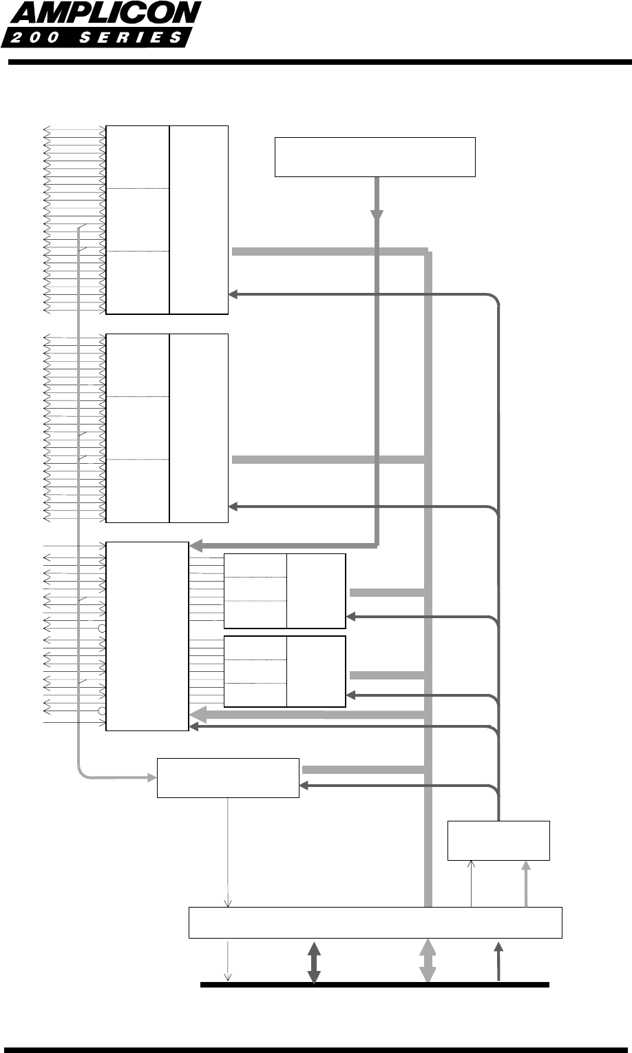
Figure 2 - PC215E Block Diagram
Port C
Port B
Port A
82C55
PPI - Y
Port
C
Port B
Port A
82C55
PPI - X
CTR 2
CTR 1
CTR 0
Address Offset
Decoder
Interrupts Enable and
Status Registers
W/R
5 bit Address
Offset
Event
Interrupt
8 bit
Data
I/O
Bus
82C54
Ctr/Tmr
Z2
82C54
Ctr/Tmr
Z1
CTR 2
C
TR 1
CTR 0
AddressControls DataIRQ
ISA Bus
PC INTERFACE
A0
A1
A2
A3
A4
A5
A6
A7
C0
C1
C2
C3
C4
C5
C6
C7
B0
B1
B2
B3
B4
B5
B6
B7
A0
A1
A2
A3
A4
A5
A6
A7
C0
C1
C2
C3
C4
C5
C6
C7
B0
B1
B2
B3
OUT0
GAT0
Z1 I/P
Z2 I/P
CLK0
B4
B5
B6
B7
OUT1
GAT1
CLK1
/OUT0
OUT2
GAT2
CLK2
OUT0
GAT0
CLK0
OUT1
GAT1
CLK1
/OUT0
OUT2
GAT2
CLK2
Counter
Connection
Registers
Z1 and Z2
Board Crystal Clock Generator
(5 source frequencies)