ACM8068 Quad band GSM/GPRS Module Hardware Application Note AMOD Technology Co.,LTD Subject to changes in technology, design and availability URL: http://www.amod.com.tw Add. 8F., No. 46, Lane 10, Jihu Road, Neihu, Taipei 11492, Taiwan, R.O.C. Tel. +886-2-8751-6263; Fax +886-2-8751-6755; Email sales@amod.com.
Date: 2010/02/04 Version: 1.0 Status: Released Change History Version V1.0 2/22 Effective Date Description of Changes 2010/02/04 Released ACM8068 HW Application Manual V1.
Date: 2010/02/04 Version: 1.0 Status: Released Table of Contents TABLE OF CONTENTS ....................................................................................................................... 3 LIST OF TABLES ................................................................................................................................. 4 LIST OF FIGURES ............................................................................................................................... 4 1.
Date: 2010/02/04 Version: 1.0 Status: Released List of Tables Table 1: ACM8068 key feature list ................................................................................ 5 Table 2: UART Data configuration.............................................................................. 10 Table 3: UART0 pin out description ............................................................................ 10 Table 4: UART1 pin out connector ......................................................................
Date: 2010/02/04 Version: 1.0 Status: Released 1. ACM8068 Key Features Table 1: ACM8068 key feature list Product features 48PIN SMD pad SIM interface Audio interface Descriptions GSM 850/ GSM900/GSM1800 /GSM1900 Quad Band GSM850/EGSM900 Class4 (2W) GSM1800 GSM 1900 Class1 (1W) 850/900 <-109dBm 1800/1900 <-105~106dBm -30°C~+85°C 3.4V~4.5V (4.0V is recommended) <2mA (Standby mode) <0.1mA Support GSM/GPRS Phase2/2+ GSM Standard AT COMMAND V.
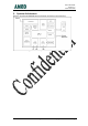
Date: 2010/02/04 Version: 1.0 Status: Released 2. System Architecture Figure 1 describes ACM8068 function diagram and main system interface. UART1 UART0 Figure 1: ACM8068 system function block diagram 6/22 ACM8068 HW Application Manual V1.
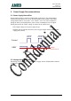
Date: 2010/02/04 Version: 1.0 Status: Released 3. Power Supply Recommendations 3.1 Power Supply Generalities Power supply design is critical to GSM module applications. The design guides should be strictly followed to ensure the performance of the module. The VBAT voltage limits must be at any time: 3.4V
Date: 2010/02/04 Version: 1.0 Status: Released Figure 3: Voltage drop versus distance 3.3 Design Recommendation Additional notes to the design of power supply circuit: • Quality attention must be paid to the power supply circuit for their resistance value and burst current. • The circuit line between power supply input to VBAT should try to avoid interference of other source of signals. • Decoupling capacitors. 3.3.
Date: 2010/02/04 Version: 1.0 Status: Released 4. Interfaces 4.1UART Interface 4.1.1 UART interface characteristic and pin out description ACM8068 has two UARTs. UART0 is used to communicate with host systems, and to download the memory FLASH.
Date: 2010/02/04 Version: 1.0 Status: Released ESD SIM Figure 9: SIM connector layout reference 4.3.3 SIM Card Interface 1 5 2 6 3 7 Top view Table 6: SIM connector pin out Pin number Schematics name Description 1 SIM_VCC Supply voltage (1.8 or 3V) 2 SIMRSCDn_ESD Reset for SIM card 3 SIMCKCDn_ESD Clock for SIM card 5 GND Ground 6 SIM_VCC Supply voltage (1.8 or 3V) 7 SIMIOCD_ESD I/O line to/from SIM card 4.
Date: 2010/02/04 Version: 1.0 Status: Released Figure 10: RF Interface Design 15/22 ACM8068 HW Application Manual V1.
Date: 2010/02/04 Version: 1.0 Status: Released 4.5 LED Indicators PIN 5 and PIN 13 can be used as system indicators (refer to enhanced AT command for function switch): PIN 5: When the output is at high level, the system is ready to accept AT command. V4.0 LED3 GREEN R15 220R R18 10K Q1 2N3904 LPG_GREEN R60 10K Figure 11: PIN 5 for system ready indication PIN 13: When the output is at high level, the module had camped on the network. V4.
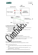
Date: 2010/02/04 Version: 1.0 Status: Released 5. Power ON/OFF Procedure It is recommended to use following procedure to power on/off module. Follow below procedure as described as figure 1: Figure 13: Before Power-In, ONKEY has been in the “Low” mode Figure 14: Before Power-In, ONKEY is not in “Low” mode 17/22 ACM8068 HW Application Manual V1.
Date: 2010/02/04 Version: 1.0 Status: Released Figure 15: GSM Sleep Process 18/22 ACM8068 HW Application Manual V1.
Date: 2010/02/04 Version: 1.0 Status: Released 6. Electrical & Environmental Characteristics Table 7: MIC 1 audio input electrical requirements Parameter Typical Value Maximum input level (MIC+–MIC-) 32.5mVrms Differential input resistance (MICI+–MICI-) MIC Skew voltage 220 KΩ 1.9~2.1V 2.0~2.
Date: 2010/02/04 Version: 1.0 Status: Released 7. Appendix 1.
Date: 2010/02/04 Version: 1.0 Status: Released Power input positive, input voltage is limited to 3.5V ~ 4.5V 38 VBAT 39 VBAT 40 GPO1 41 NETLIGHT 42 DCD UART0 DCD 43 DTR UART0 DTR 44 RTS UART0 RTS 45 CTS UART0 CTS 46 GPIO General purpose I/O 47 SIM_PRESENCE SIM interface 48 GND Ground Power input positive, input voltage is limited to 3.5V ~ 4.5V General purpose I/O ACM8068 module is used as DCE (Data circuit-terminating equipment).
Date: 2010/02/04 Version: 1.0 Status: Released 8. Appendix 2. PCB PAD Land Pattern ACM8068 is a 48 Pin PCB PAD with 0.5mm pitch as pig 2-1 and the dimension is 33mm x 33mm x 3.3mm (high). The model number is Hirose’s DF12C(3.0)-50DS-0.5V. The pad is as figure 16. Figure 16: 48 pin SMD pad 22/22 ACM8068 HW Application Manual V1.
FCC Regulations: This device complies with part 15 of the FCC Rules. Operation is subject to the following two conditions: (1) This device may not cause harmful interference, and (2) this device must accept any interference received, including interference that may cause undesired operation. This device has been tested and found to comply with the limits for a Class B digital device, pursuant to Part 15 of the FCC Rules.