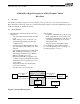
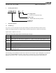
AMD-8151TM AGP Tunnel Data Sheet 24888 Rev 3.03 - July 12, 2004 TM AMD-8151 Cover page HyperTransportTM AGP3.0 Graphics Tunnel Data Sheet 1 Overview The AMD-8151TM HyperTransportTM AGP3.0 Graphics Tunnel (referred to as the IC in this document) is a HyperTransport™ technology (referred to as link in this document) tunnel developed by AMD that provides an AGP 3.0 compliant (8x transfer rate) bridge. 1.1 • Device Features HyperTransport technology tunnel with side A and side B.
4888 Rev 3.03 - July 12, 2004 AMD-8151TM AGP Tunnel Data Sheet © 2004 Advanced Micro Devices, Inc. All rights reserved.The contents of this document are provided in connection with Advanced Micro Devices, Inc. ("AMD") products. AMD makes no representations or warranties with respect to the accuracy or completeness of the contents of this publication and reserves the right to make changes to specifications and product descriptions at any time without notice.
24888 Rev 3.03 - July 12, 2004 AMD-8151TM AGP Tunnel Data Sheet Table of Contents 1 Overview . . . . . . . . . . . . . . . . . . . . . . . . . . . . . . . . . . . . . . . . . . . . . . . . . . . . . . . . . . . . . . . . . . . . . . . 1 1.1 Device Features. . . . . . . . . . . . . . . . . . . . . . . . . . . . . . . . . . . . . . . . . . . . . . . . . . . . . . . . . . . . . . 1 2 Ordering Information. . . . . . . . . . . . . . . . . . . . . . . . . . . . . . . . . . . . . . . . . . . . . . . . . . . .
24888 Rev 3.03 - July 12, 2004 AMD-8151TM AGP Tunnel Data Sheet List of Figures Figure 1: Figure 2: Figure 3: Figure 4: Figure 5: System block diagram................................................................................................................... 1 Configuration space. ................................................................................................................... 14 Ball designations. ..................................................................................
24888 Rev 3.03 - July 12, 2004 AMD-8151TM AGP Tunnel Data Sheet List of Tables Table 1: Table 2: Table 3: Table 4: Table 5: Table 6: Table 7: Table 8: Table 9: Table 10: Table 11: Table 12: Table 13: Table 14: Table 15: Table 16: Table 17: IO signal types. ............................................................................................................................. 6 Translation from AGP requests to link requests. ........................................................................
AMD-8151TM AGP Tunnel Data Sheet 24888 Rev 3.03 - July 12, 2004 2 Ordering Information AMD-8151 BL C Case Temperature C = Commercial temperature range Package Type BL = Organic Ball Grid Array with lid Family/Core AMD-8151 3 Signal Descriptions 3.1 Terminology See section 5.1.2 for a description of the register naming convention used in this document. See the AMD-8151TM HyperTransportTM AGP3.0 Graphics Tunnel Design Guide for additional information. Signals with a # suffix are active low.
24888 Rev 3.03 - July 12, 2004 3.2 AMD-8151TM AGP Tunnel Data Sheet Tunnel Link Signals The following are signals associated with the HyperTransportTM links. [B, A] in the signal names below refer to the A and B sides of the tunnel. [P, N] are the positive and negative sides of differential pairs. Pin name and description IO cell Power During After type plane* reset reset LDTCOMP[3:0]. Link compensation pins for both sides of the tunnel.
AMD-8151TM AGP Tunnel Data Sheet 24888 Rev 3.03 - July 12, 2004 3.3 AGP Signals In the table below, “Term” indicates the standard AGP 3.0 termination impedance to ground; “PU” indicates a weak pullup resistor; “PD” indicates a weak pulldown resistor. Pin name and description IO cell Power type plane AGP 3.0 Signaling AGP 2.0 Signaling During After During After reset reset reset reset A_ADSTB0_[P, N]. AGP differential strobe for A_AD[15:0] and A_CBE_L[1:0]. When AGP 3.
AMD-8151TM AGP Tunnel Data Sheet 24888 Rev 3.03 - July 12, 2004 Pin name and description IO cell Power type plane AGP 3.0 Signaling AGP 2.0 Signaling During After During After reset reset reset reset A_GNT#. AGP master grant signal. Low PU High Term PU PU Low Low Low Low VDD15 Term Term PU Low A_PCLK. 66 MHz AGP clock. Output VDD33 Func. Func. Func. Func. A_PLLCLKO. PLL clock output. See section 4.3 for details. Output VDD33 Func. Func. Func. Func.
24888 Rev 3.03 - July 12, 2004 3.4 AMD-8151TM AGP Tunnel Data Sheet Test and Miscellaneous Signals Pin name and description CMPOVR. Link automatic compensation override. 0=Link automatic compensation is enabled. 1=The compensation values stored in DevA:0x[E0, E4, E8] control the compensation circuit. The state of this signal determines the default value for DevA:0x[E0, E4, E8][ACTL and BCTL] at the rising edge of PWROK. IO cell Power During After type plane reset reset Input VDD33 FREE[7:1].
24888 Rev 3.03 - July 12, 2004 4 Functional Operation 4.1 Overview AMD-8151TM AGP Tunnel Data Sheet The IC connects to the host through either the side A or side B HyperTransportTM link interface. The other side of the tunnel may or may not be connected to another device. Host-initiated transactions that do not target the IC or the bridge flow through the tunnel to the downstream device. Transactions claimed by the device are passed to internal registers or to the AGP bridge. See section 5.
24888 Rev 3.03 - July 12, 2004 AMD-8151TM AGP Tunnel Data Sheet In summary, Stop Grant broadcasts with SMAF fields specified by DevA:0xF0[ICGSMAF] enable the clock gating window and STPCLK deassertion broadcasts disable the window. If LDTSTOP# is asserted while the clock gating window is enabled, then clock gating occurs. Also, DevA:0xF0[ECGSMAF] may be used in a similar way to disable A_PCLK and the internal clock grids associated with the AGP bridge.
24888 Rev 3.03 - July 12, 2004 AMD-8151TM AGP Tunnel Data Sheet All AGP transactions are compliant to AGP ordering rules.
AMD-8151TM AGP Tunnel Data Sheet 24888 Rev 3.03 - July 12, 2004 The first calibration cycle occurs approximately 4 milliseconds after the deassertion of RESET# (whether AGP 2.0 or 3.0 signaling is enabled). 5 Registers 5.1 Register Overview The IC includes several sets of registers accessed through a variety of address spaces. IO address space refers to register addresses that are accessed through x86 IO instructions such as IN and OUT.
AMD-8151TM AGP Tunnel Data Sheet 24888 Rev 3.03 - July 12, 2004 The following are configuration spaces: Device Function Mnemonic Registers "A" 0 DevA:0xXX AGP device header; link and AGP capabilities blocks "B" 0 DevB:0xXX PCI-PCI bridge registers for AGP Table 3: Configuration spaces. The IC does not claim configuration-register accesses to unimplemented functions within its devices (they are forwarded to the other side of the tunnel).
AMD-8151TM AGP Tunnel Data Sheet 24888 Rev 3.03 - July 12, 2004 AGP Device Status And Command Register Default: 0210 0000h Bits Description DevA:0x04 Attribute: See below. 31 DPE: detected parity error. Read only. This bit is fixed in the low state. 30 SSE: signaled system error. Read; set by hardware; write 1 to clear. 1=A system error was signaled (both links were flooded with sync packets) as a result of a CRC error (see DevA:0x[C8:C4][CRCFEN, CRCERR]).
AMD-8151TM AGP Tunnel Data Sheet 24888 Rev 3.03 - July 12, 2004 AGP Device Graphic Virtual Memory Aperture Register DevA:0x10 It is expected that the state of this register is copied into the host by software. This register controls no hardware in the IC. Default: 0000 0000 0000 0008h Bits Description Attribute: See below. 63:32 APBARHI. Read-write. Aperture base address register high. Note: bits[63:40] are required to be programmed low; setting any of these bits high results in undefined behavior.
24888 Rev 3.03 - July 12, 2004 AMD-8151TM AGP Tunnel Data Sheet AGP Miscellaneous Control Register Default: 0000 0000h Bits Description DevA:0x40 Attribute: See below. 31:8 Reserved. 7 Must be low. This bit is required to be low at all times; setting it high results in undefined behavior. 6 Must be low. This bit is required to be low at all times; setting it high results in undefined behavior. 5 Must be low. This bit is required to be low at all times; setting it high results in undefined behavior.
24888 Rev 3.03 - July 12, 2004 AMD-8151TM AGP Tunnel Data Sheet AGP PHY Control Register DevA:0x[54, 50] These registers apply to the compensation values of AGP clock-forwarded data and strobe signals as follows: • DevA:0x50: data signals A_AD[31:0], A_CBE_L[3:0], A_DBI[H, L], and A_SBA[7:0]. • DevA:0x54: strobe signals A_ADSTB[1:0]_[P, N] and A_SBSTB_[P, N].
AMD-8151TM AGP Tunnel Data Sheet 24888 Rev 3.03 - July 12, 2004 15:14 PCTL: AGP PHY P (rising edge) compensation control. Read-write. These two bits combine to specify the PHY rising edge compensation value that is applied to AGP signals as follows: PCTL 00b 01b 10b 11b Description Apply PCOMP directly as the compensation value. Apply PDATA directly as the compensation value. Apply the sum of PCOMP and PDATA as the compensation value. If the sum exceeds 1Fh, then 1Fh is applied.
AMD-8151TM AGP Tunnel Data Sheet 24888 Rev 3.03 - July 12, 2004 AGP Most Recent Request Register DevA:0x60 As each PIPE mode or SBA mode AGP request is transferred into the IC, the fields are placed into this register. Thus, this register provides the fields of the most recent AGP requests. Any sticky bits from prior requests that have not been updated in the current request are also valid. Note: fences are not captured by this register.
24888 Rev 3.03 - July 12, 2004 AMD-8151TM AGP Tunnel Data Sheet 4 FWSUP: fast write support flag. 0=Fast writes are not supported. 1=Fast writes are supported. The state of this bit is controlled by DevA:0x40[FWDIS]. 3 AGP3MD: AGP 3.0 signaling mode detected. 1=The IC detected connection to an AGP 3.0-capable master and is programmed for AGP 3.0 signaling. 0=The IC detected connection to an AGP 2.0 or earlier capable master or is not programmed for 1.5-volt, AGP 2.0 signaling.
AMD-8151TM AGP Tunnel Data Sheet 24888 Rev 3.03 - July 12, 2004 2:0 DRATE: data transfer mode rate. This field is combined with DevA:0xA4[AGP3MD] to specify the AGP data rate as follows: AGP3MD X 0 0 0 1 1 1 DRATE 000 001 010 100 001 010 100 No AGP mode selected. 1x AGP rate; AGP 2.0 signaling. 2x AGP rate; AGP 2.0 signaling. 4x AGP rate; AGP 2.0 signaling. 4x AGP rate; AGP 3.0 signaling. 8x AGP rate; AGP 3.0 signaling. Reserved.
AMD-8151TM AGP Tunnel Data Sheet 24888 Rev 3.03 - July 12, 2004 11:0 APSIZE: graphic virtual memory aperture size. Read-write (except bits[11, 7:6, and 2:0] which are read only, fixed at the default value). This field specifies the size of the aperture pointed to by DevA:0x10. This field also controls read only versus read-write control over several bits in DevA:0x10.
24888 Rev 3.03 - July 12, 2004 26 AMD-8151TM AGP Tunnel Data Sheet MASHST: master host. Read; set and cleared by hardware. This bit indicates which link is the path to the master (or only) host bridge on the HyperTransport™ technology chain. 1=The hardware set this bit as a result of a write command from the B side of the tunnel to any of the bytes of DevA:0xC0[31:16]. 0=The hardware cleared this bit as a result of a write command from the A side of the tunnel to any of the bytes of DevA:0xC0[31:16].
24888 Rev 3.03 - July 12, 2004 AMD-8151TM AGP Tunnel Data Sheet 18:16 Max link width in. Read only. This specifies the width of the incoming link to be 16 bits wide for side A and 8 bits wide for side B. 15 Reserved. 14 EXTCTL: extended control time during initialization. Read-write. This specifies the time in which LT[B, A]CTL is held asserted during the initialization sequence that follows an LDTSTOP# deassertion, after LR[B, A]CTL is detected asserted. 0=At least 16 bit times.
24888 Rev 3.03 - July 12, 2004 AMD-8151TM AGP Tunnel Data Sheet Link Frequency Capability 0 Register Default: 0035 0022h. Bits Description DevA:0xCC Attribute: See below. 31:16 FREQCAPA: link A frequency capability. Read only. These bits indicate that A side of the tunnel supports 200, 400, 600, and 800 MHz link frequencies. 15:12 Reserved. 11:8 FREQA: link A frequency. Read-write. Specifies the link side A frequency. Legal values are 0h (200 MHz), 2h (400 MHz), 4h (600 MHz), and 5h (800 MHz).
24888 Rev 3.03 - July 12, 2004 AMD-8151TM AGP Tunnel Data Sheet Link PHY Compensation Control Registers DevA:0x[E8, E4, E0] The link PHY circuitry includes automatic compensation that is used to adjust the electrical characteristics for the link transmitters and receivers on both sides of the tunnel. There is one compensation circuit for the receivers and one for each polarity of the transmitters.
24888 Rev 3.03 - July 12, 2004 6:5 AMD-8151TM AGP Tunnel Data Sheet ACTL: link side A PHY control value. Read-write. These two bits combine to specify the PHY compensation value that is applied to side A of the tunnel as follows: ACTL 00b 01b 10b 11b Description Apply CALCCOMP directly as the compensation value. Apply ADATA directly as the compensation value. Apply the sum of CALCCOMP and ADATA as the compensation value. In DevA:0x[E4, E0], if the sum exceeds 13h, then 13h is applied.
AMD-8151TM AGP Tunnel Data Sheet 24888 Rev 3.03 - July 12, 2004 5.3 AGP Bridge Configuration Registers These registers are located in PCI configuration space, in the second device (device B), function 0. See section 5.1.2 for a description of the register naming convention. AGP Bridge Vendor And Device ID Register Default: 7455 1022h Bits Description DevB:0x00 Attribute: See below. 31:16 AGP bridge device ID. Bits[31:20] are read only; bits[19:16] are write-once.
AMD-8151TM AGP Tunnel Data Sheet 24888 Rev 3.03 - July 12, 2004 15:8 LATENCY. Read-write. These bits control no hardware. 7:0 CACHE. Read only. These bits fixed at their default values. AGP Bridge Bus Numbers And Secondary Latency Register Default: 0000 0000h Bits Description DevB:0x18 Attribute: Read-write. 31:24 SECLAT. Secondary latency timer. These bits control no hardware. 23:16 SUBBUS. Subordinate bus number. 15:8 SECBUS. Secondary bus number. 7:0 PRIBUS. Primary bus number.
AMD-8151TM AGP Tunnel Data Sheet 24888 Rev 3.03 - July 12, 2004 • Host-initiated transactions inside the windows are routed to the AGP bus. • PCI transactions initiated on the AGP bus inside the windows are not claimed by the IC. • Host initiated transactions outside the windows are passed through the tunnel or master aborted if the IC is at the end of a HyperTransport technology chain.
24888 Rev 3.03 - July 12, 2004 DevB:0x24. Default: 0000 FFF0h Bits Description AMD-8151TM AGP Tunnel Data Sheet Attribute: Read-write. 31:20 PMEMLIM. Prefetchable memory limit address bits[31:20]. See DevB:0x[30:1C] above. 19:16 Reserved. 15:4 PMEMBASE. Prefetchable memory base address bits[31:20]. See DevB:0x[30:1C] above. 3:0 Reserved. DevB:0x30. Default: 0000 FFFFh Bits Description Attribute: Read-write. 31:16 IOLIM. IO limit address bits[31:16]. See DevB:0x[30:1C] above. 15:0 IOBASE.
AMD-8151TM AGP Tunnel Data Sheet 24888 Rev 3.03 - July 12, 2004 6 Electrical Data 6.1 Absolute Ratings The IC is not designed to operate beyond the parameters shown in the following table. Parameter Minimum Maximum VDD12[B, A] –0.5 V 1.7 V VDD15 –0.5 V 2.0 V VDD18, VDDA18 –0.5 V 2.3 V VDD33 –0.5 V 3.6 V 85 °C TCASE (Under Bias) TSTORAGE Comments -65 °C 150 °C Table 6: Absolute maximum ratings. 6.
AMD-8151TM AGP Tunnel Data Sheet 24888 Rev 3.03 - July 12, 2004 6.3 DC Characteristics See the HyperTransportTM Technology Electrical Specification for the DC characteristics of link signals. The following table shows current consumption in amps and power in watts for each power plane. Typical Max Supply Parameter Description Current Power Current Power VDD12 VDD12[B, A] current, power 0.21 A 0.25 W 0.27 A 0.34 W VDD15 VDD15 current, power 0.05 A 0.08 W 0.08 A 0.
AMD-8151TM AGP Tunnel Data Sheet 24888 Rev 3.03 - July 12, 2004 The following table shows DC characteristics for signals on the VDD15 power plane when AGP 2.0 signaling is enabled. Symbol Parameter Description Min Max Units VIL Input low voltage -0.5 0.4 VDD15 V VIH Input high voltage 0.6 VDD15 0.5 + VDD15 V VOL Output low voltage; IOUT = 1.0 mA VOH Output high voltage; IOUT = 0.2 mA 0.85 VDD15 VREFI Input reference voltage on A_REFGC 0.48 VDD15 0.
AMD-8151TM AGP Tunnel Data Sheet 24888 Rev 3.03 - July 12, 2004 6.4 AC Characteristics See the HyperTransport Technology Electrical Specification for the AC characteristics of link signals. The following table shows AC specification data for clocks.
AMD-8151TM AGP Tunnel Data Sheet 24888 Rev 3.03 - July 12, 2004 The following table shows AC specification data for clock-forwarded operation of AGP signals. AGP 2X AGP 4X AGP 8X Symbol Parameter Description Min Max Min Max Min Max Units tTSF A_PCLK to transmit strobe first strobe edge tTSR A_PCLK to transmit strobe final strobe edge tDVB Data valid before strobe 1.7 -0.95 0.527 ns tDVA Data valid after strobe 1.9 1.15 0.
AMD-8151TM AGP Tunnel Data Sheet 24888 Rev 3.
AMD-8151TM AGP Tunnel Data Sheet 24888 Rev 3.03 - July 12, 2004 Alphabetical listing of signals and corresponding BGA designators.
AMD-8151TM AGP Tunnel Data Sheet 24888 Rev 3.
AMD-8151TM AGP Tunnel Data Sheet 24888 Rev 3.03 - July 12, 2004 8 Package Specification A1 CORNER D A1 CORNER D1 D3 Øb (Nx Plcs) E3 E2 E E1 e D2 BOTTOM VIEW TOP VIEW LID NOT TO SCALE A2 SEE NOTES A SIDE VIEW A1 AMD PACKAGE SYMBOL GENERAL NOTES D/E D1/E1 1. All dimensions are specified in millimeters (mm). 2. Dimensioning and tolerancing per ASME-Y14.5M-1994. 3.
AMD-8151TM AGP Tunnel Data Sheet 24888 Rev 3.03 - July 12, 2004 9 Test The IC includes the following test modes. Mode TEST A_TYPEDET LDTSTOP# STRAPL0 Notes Operational 0 X X X High impedance 1 0 0 0 NAND tree 1 0 0 1 Table 17: Test modes. 9.1 High Impedance Mode In high-impedance mode, all the signals of the IC are placed into the high-impedance state. 9.2 NAND Tree Mode There are several NAND trees in the IC. Some of the inputs are differential (e.g.
AMD-8151TM AGP Tunnel Data Sheet 24888 Rev 3.03 - July 12, 2004 NAND tree 1: output signal is STRAPL[5]. However, the gate connected to the last signal in this NAND tree (LDTCOMP[3]) is an AND gate rather than a NAND gate; so the expected output of this NAND tree is inverted compared to the other NAND trees.
AMD-8151TM AGP Tunnel Data Sheet 24888 Rev 3.03 - July 12, 2004 NAND tree 3: output signal is STRAPL[3].