
User Guide


120 128-Bit Media and Scientific Programming
AMD64 Technology 24592—Rev. 3.15—November 2009
• 10 = round up
• 11 = round toward zero
For details, see “Floating-Point Rounding” on page 132.
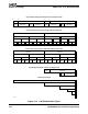
Flush-to-Zero (FZ). Bit 15. If the rounded result is tiny and the underflow mask is set, the FTZ bit
causes the result to be flushed to zero. This naturally causes the result to be inexact, which causes both
PE and UE to be set. The sign returned with the zero is the sign of the true result. The FTZ bit does not
have any effect if the underflow mask is 0.
This response does not comply with the IEEE 754 standard, but it may offer higher performance than
can be achieved by responding to an underflow in this circumstance. The FZ bit is only effective if the
UM bit is set to 1. If the UM bit is cleared to 0, the FZ bit is ignored. For details, see Table 4-14 on
page 185.
Misaligned Exception Mask (MM). Bit 17. If the misaligned exception mask (MM) is set to 1, a 16-
byte misaligned memory access on most packed SSE instructions will not cause a #GP exception, but
will be subject to alignment checking (#AC) instead. When MM is set and alignment-checking is
enabled, a #AC exception is generated, if the memory operand is not 16-byte aligned. The
corresponding MXCSR_MASK bit (17) is 1, regardless of whether MM is set or not. For details on
MXCSR and MXCSR_MASK, see “128-Bit, 64-Bit, and x87 Programming” in the AMD64
Architecture Programmer’s Manual Volume 2: System Programming, order #24593. For details on
alignment handling, see “Data Alignment” on page 123.
Support for misaligned SSE mode is indicated by ECX bit 7 of CPUID function 8000_0001h.
4.3.3 Other Data Registers
Some 128-bit media instructions that perform data transfer, data conversion or data reordering
operations (“Data Transfer” on page 135, “Data Conversion” on page 139, and “Data Reordering” on
page 140) can access operands in the MMX or general-purpose registers (GPRs). When addressing
GPRs registers in 64-bit mode, the REX instruction prefix can be used to access the extended GPRs, as
described in “REX Prefixes” on page 74.
For a description of the GPR registers, see “Registers” on page 23. For a description of the MMX
registers, see “MMX™ Registers” on page 200.
4.3.4 rFLAGS Registers
The COMISS, COMISD, UCOMISS, and UCOMISD instructions, described in “Compare” on
page 171, write flag bits in the rFLAGS register. For a description of the rFLAGS register, see “Flags
Register” on page 33.