
User Guide

General-Purpose Programming 97
24592—Rev. 3.15—November 2009 AMD64 Technology
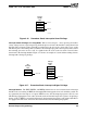
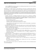
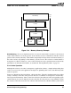
Figure 3-19. Memory Hierarchy Example
Write Buffering. Processor implementations can contain write-buffers attached to the internal
caches. Write buffers can also be present on the interface used to communicate with the external
portions of the memory hierarchy. Write buffers temporarily hold data writes when main memory or
the caches are busy responding to other memory-system accesses. The existence of write buffers is
transparent to software. However, some of the instructions used to optimize memory-hierarchy
performance can affect the write buffers, as described in “Forcing Memory Order” on page 94.
3.9.4 Cache Operation
Although the existence of caches is transparent to application software, a simple understanding how
caches are accessed can assist application developers in optimizing their code to run efficiently when
caches are present.
Caches are divided into fixed-size blocks, called cache lines. Typically, implementations have either
32-byte or 64-byte cache lines. The processor allocates a cache line to correspond to an identically-
sized region in main memory. After a cache line is allocated, the addresses in the corresponding region
of main memory are used as addresses into the cache line. It is the processor’s responsibility to keep
the contents of the allocated cache line coherent with main memory. Should another system device
513-137.eps
Processor
L3 Cache
Main Memory
L2 Cache
L1 Instruction
Cache
L1 Data
Cache
System
Faster
Access
Larger
Size