
User guide


Chapter 6: Functional Description—High-Performance Controller 6–5
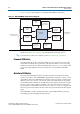
Block Description
December 2010 Altera Corporation External Memory Interface Handbook Volume 3
Section II. DDR3 SDRAM Controller with ALTMEMPHY IP User Guide
Control Logic
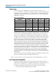
Bus commands control SDRAM devices using combinations of the
mem_ras_n
,
mem_cas_n
, and
mem_we_n
signals. For example, on a clock cycle where all three signals
are high, the associated command is a no operation (NOP). A NOP command is also
indicated when the chip select signal is not asserted. Table 6–2 shows the standard
SDRAM bus commands.
The DDR3 SDRAM HPC must open SDRAM banks before it accesses the addresses in
that bank. The row and bank to be opened are registered at the same time as the active
(ACT) command. The DDR3 SDRAM HPC closes the bank and opens it again if it
needs to access a different row. The precharge (PCH) command closes only a bank.
The primary commands used to access SDRAM are read (RD) and write (WR). When
the WR command is issued, the initial column address and data word is registered.
When a RD command is issued, the initial address is registered. The initial data
appears on the data bus 5 to 11 clock cycles later. This delay is the column address
strobe (CAS) latency and is due to the time required to read the internal DRAM core
and register the data on the bus. The CAS latency (of 6) depends on the speed of the
SDRAM and the frequency of the memory clock. In general, the faster the clock, the
more cycles of CAS latency are required. After the initial RD or WR command,
sequential reads and writes continue until the burst length is reached. DDR3 SDRAM
devices support fixed burst lengths of 4 or 8 data cycles or an on-the-fly mode where
the controller can request a burst of 4 or 8 for each read or write command. This
on-the-fly mode is the only mode supported. The auto-refresh command (ARF) is
issued periodically to ensure data retention. This function is performed by the DDR3
SDRAM HPC.
The load mode register command (LMR) configures the SDRAM mode register. This
register stores the CAS latency, burst length, and burst type.
f For more information, refer to the specification of the SDRAM that you are using.
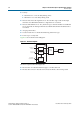
Error Correction Coding (ECC)
The optional ECC logic comprises an encoder and a decoder-corrector, which can
detect and correct single-bit errors and detect double-bit errors. The ECC logic uses an
8-bit ECC for each 64-bit message. The ECC logic has the following features:
■ Hamming code ECC logic that encodes every 64-bits of data into 72-bits of
codeword with 8-bits of Hamming code parity bits
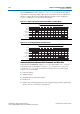
Table 6–2. Bus Commands
Command Acronym ras_n cas_n we_n
No operation NOP High High High
Active ACT Low High High
Read RD High Low High
Write WR High Low Low
Precharge PCH Low High Low
Auto refresh ARF Low Low High
Load mode register LMR Low Low Low