
User guide


6–4 Chapter 6: Functional Description—High-Performance Controller
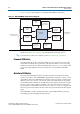
Block Description
External Memory Interface Handbook Volume 3 December 2010 Altera Corporation
Section II. DDR3 SDRAM Controller with ALTMEMPHY IP User Guide
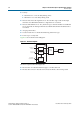
PHY Interface Logic
When the main state machine issues a write command to the memory, the write data
for that write burst has to be fetched from the write data FIFO buffer. The relationship
between write command and write data depends on the memory type, ALTMEMPHY
interface type, CAS latency, and the full-rate or half-rate setting. The PHY interface
logic adjusts the timing of the write data FIFO read request signal so that the data
arrives on the external memory interface DQ pins at the correct time.
ODT Generation Logic
The ODT generation logic (not shown in Figure 6–2) calculates when and for how
long to enable the ODT outputs. It also decides which ODT bit to enable, based on the
number of chip selects in the system.
■ 1 DIMM (1 or 2 chip selects)
In the case of a single DIMM, the ODT signal is only asserted during writes. The
ODT signal on the DIMM at
mem_cs[0]
is always used, even if the write command
on the bus is to
mem_cs[1]
. In other words,
mem_odt[0]
is always asserted even if
there are two ODT signals.
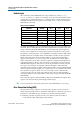
■ 2 or more DIMMs
In the multiple DIMM case, the appropriate ODT bit is asserted for both read and
writes. Table 6–1 shows which ODT signal on the adjacent DIMM is enabled.
Low-Power Mode Logic
The low-power mode logic (not shown in Figure 6–2) monitors the
local_powerdn_req
and
local_self_rfsh_req
request signals. This logic also informs
the user of the current low-power state via the
local_powerdn_ack
and
local_self_rfsh_ack
acknowledge signals.
1 HPC supports only precharge power-down mode and not active power-down mode.
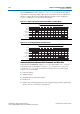
Table 6–1. ODT
Write or Read On ODT Enabled
mem_cs[0]
or
cs[1] mem_odt[2]
mem_cs[2]
or
cs[3] mem_odt[0]
mem_cs[4]
or
cs[5] mem_odt[6]
mem_cs[6]
or
cs[7] mem_odt[4]